SLVAF01 October 2020 TPS55340
1.1 Reflected Voltage, VOR
In a typical flyback converter, there is voltage which is reflected from secondary side when the primary side switch is turned off and the stored energy is transferring to the load through transformer. This reflected voltage, VOR will form voltage stress to the switching device after adding maximum input VDC, VIN in worst case. So the amplitude of the reflected voltage, VOR will be a key design factor, affecting voltage stress to the switching device.

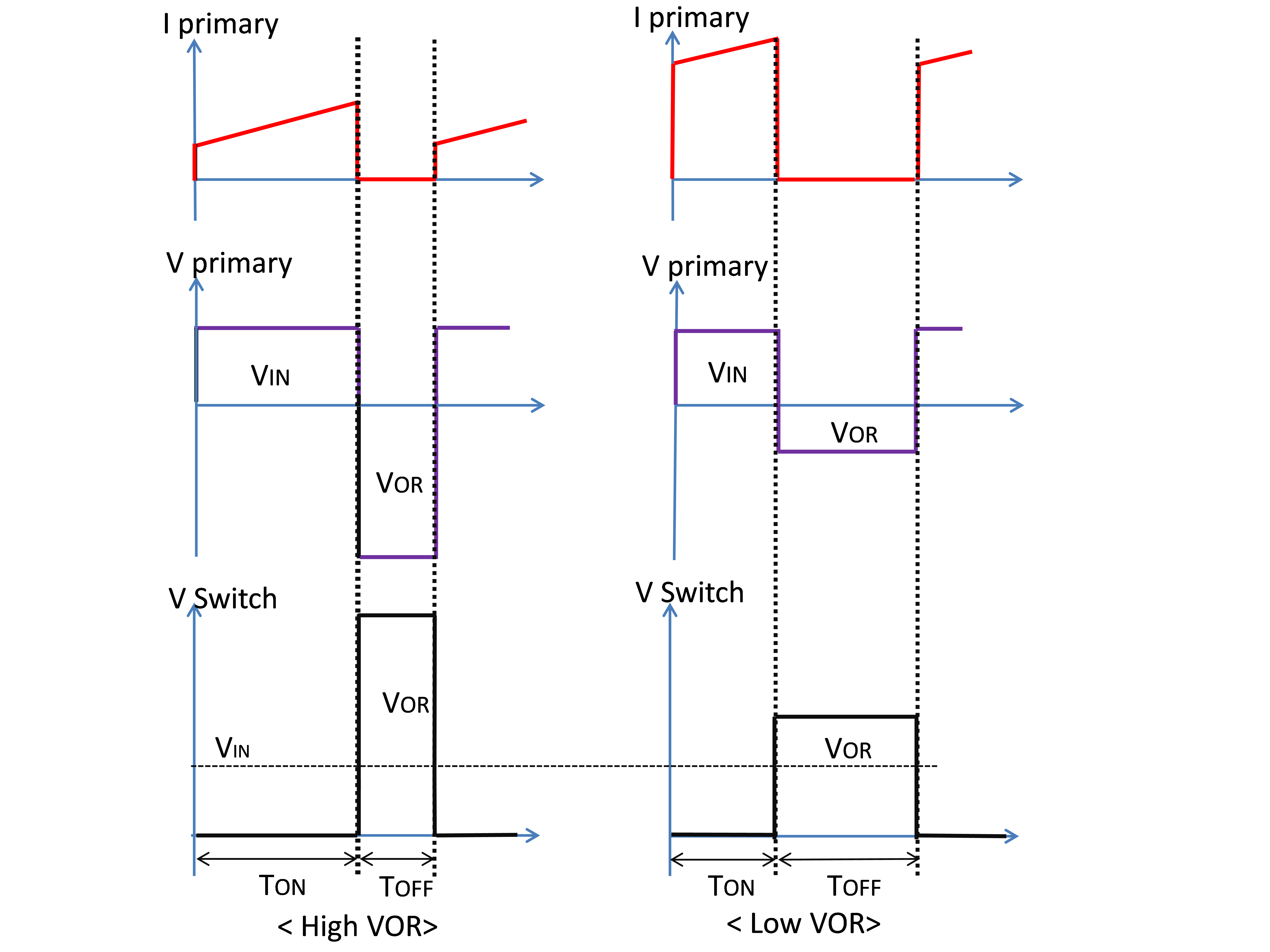
From the simple equation above, VOR is set by primary to secondary turn ratio once output voltage is set. And then Flyback controller or convert will set its’ duty ratio by inductor’s volt-sec balance if VOR is fixed. Figure 1-1 shows the comparison voltage and current stress according to VOR level.
 Figure 1-1 Flyback Converter's Primary
Side Current, Voltage, and Switch Note Voltage
Figure 1-1 Flyback Converter's Primary
Side Current, Voltage, and Switch Note VoltageBy adjusting turn ratio, VOR could be contained if it tops a limited level that is required by system. But a lower VOR will cause a higher peak current stress and make system have lower efficiency due to an increased conduction loss. Also, it is possible for higher peak to trigger internal current limit of the device which integrates FET inside.