Stability Analysis and Design of D-CAP2 and D-CAP3 Converter – Part 1: How to Select Output Capacitor
Trademarks
All trademarks are the property of their respective owners.
1 Introduction
D-CAP series control schemes are widely used in notebook, server, EP power and many other areas due to the advantages of good dynamic performance and less external components [1 and 2]. Different from the compensation with error amplifier in voltage mode and current mode, the zero formed by output capacitor ESR is used for loop compensation in the original D-CAP control [3 and 4]. With ESR zero after LC double poles, the slope of loop gain magnitude becomes -20dB/decade at crossover frequency, which ensures the system phase margin. For the application with MLCC or other small ESR capacitor, external or internal ripple injection circuit can be used to generate a zero instead of the ESR zero in D-CAP/D-CAP2/D-CAP3 control [5 and 6]. But if the inductor and output capacitor are not chosen properly and crossover frequency is lower than the frequency of ripple injection zero, a -40dB/decade slope at crossover frequency will happen and cause insufficient phase margin. An application design method is proposed for D-CAP2/D-CAP3 buck converter in this application report to ensure enough phase margin and system stability.
2 Open Loop Frequency Response of D-CAP2 and D-CAP3 Converter
 Figure 2-1 Control Diagram of D-CAP2
Converter
Figure 2-1 Control Diagram of D-CAP2
ConverterDiagram of buck converter with D-CAP2 control scheme is shown as Figure 2-1 . The open loop transfer function was derived in application report [2], as shown in Equation 1.

where Gdv(s) is the transfer function from Duty to Vo, well known using state-space averaging model.
Hd(s) =e-sTon/2: Delay factor of fixed on time
Tc: Time constant block of ripple injection circuit in D-CAP2
Acp: Voltage compression block of ripple injection circuit in D-CAP2
HFB(s): Transfer function of feedback divider network
The expression of Gdv(s) is shown as Equation 2.

where

RL is the load resistance, rL is DC resistance of the inductor, rc is ESR of output capacitor.
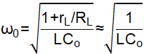
A pair of double poles (conjugate poles) and a zero formed by ESR of output capacitor are included in the transfer function Gdv(s). The angular frequency of the double poles and the zero formed by ESR are shown as Equation 4 and Equation 5.

A zero is formed by the time constant block of ripple injection in D-CAP2 control mode, the angular frequency of the zero is:

ωesr is at high frequency range in most cases. ω0 and ωRI are the dominant poles and zero to determine bandwidth and phase margin. The bode plot of open loop transfer function for D-CAP2 converter is shown as Figure 2-2.
 Figure 2-2 Bode plot of D-CAP2 Converter
To enhance DC accuracy of output voltage, D-CAP3 is proposed and widely used in TI’s current products. Compared with D-CAP2, the DC error correction performance is further improved in D-CAP3. By adding additional poles and zeros at low frequency range, the gain at low frequency range is increased to achieve better ability for DC error correction. But the characteristics of gain and phase at middle frequency and high frequency are almost same as D-CAP2 converter. The bode plot of open loop transfer function is shown as Figure 2-3.
 Figure 2-3 Bode plot of D-CAP3 Converter
Phase margin is the phase at crossover frequency and it is one of the most important value for system stability evaluation. Since the crossover frequency is at middle frequency or high frequency, the impacts of additional zeros and poles at low frequency in D-CAP3 control mode on stability analysis can be ignored. Thus the application design method for D-CAP3 stability is same as that of D-CAP2. The analysis and design method in this application report can be applied on converters using either D-CAP2 or D-CAP3 control.
3 Method to Choose LC Value for Loop Stability
For system loop stability, a -20dB/decade slope near crossover frequency is ideal for loop gain, since that can bring sufficient phase margin [7].