SLVAF47 March 2021 TPS7H4001-SP
2 DC Regulation
One obvious factor related to DC regulation is the DC setpoint accuracy of the converter supplying VCCINT. This DC accuracy depends on factors such as the accuracy of the converter’s internal reference, the passives used with the converter (such as feedback resistors) and the layout of the printed circuit board (such as ohmic drops). From these factors, the internal reference of the converter represents a large percentage of the voltage accuracy specified by the FPGA manufacturer. However, you should calculate the accuracy of the internal reference in a way that is representative of the application.
As an example, temperature heavily influences the voltage drift of a reference; thus, you should calculate the accuracy for the temperature range to which the devices will be exposed during the mission. Typically, this range is from –40°C to +90°C, which is smaller than the standard military temperature range of –55°C to +125°C used to characterize space-rated devices. The TPS7H4001-SP from Texas Instruments has an internal reference with ±1.5% accuracy across electrical and radiation conditions for the entire military temperature range. A simple calculation of the temperature coefficient (0.1 mV/°C) reveals that in the actual application (–40°C to +90°C), the accuracy of the internal reference is about ±1.1%. You must also take into account radiation effects that could potentially affect DC regulation.
DC regulation typically refers only to the DC setpoint accuracy of the converter supplying VCCINT. The XQRKU060, as well as the converters that provide its power, is offered in a ceramic package because of its use in space applications. While ceramic packages offer hermeticity, they also present unique challenges not encountered in commercial-rated devices, including a larger footprint and larger resistance given the materials used in the package. In the case of the XQRKU060, the effect of ceramic package resistance in DC regulation is larger as the current increases, and the current will depend on the bitstream used. To mitigate this larger resistance, the XQRKU060 offers two pins, VCCINT_SENSE and GND_SENSE. Figure 2-1shows the connections needed between the TPS7H4001-SP and the XQRKU060 sensing pins, as well as a simple representation of the internal package resistance for VCCINT and GND.
 Figure 2-1 XQRKU060 Sensing Connections
to the TPS7H4001-SP
Figure 2-1 XQRKU060 Sensing Connections
to the TPS7H4001-SPBecause the TPS7H4001-SP does not offer a GND sensing pin, using only the VCCINT_SENSE pin in the XQRKU060 for the feedback signal (VSENSE) compensates for the voltage drop created by the package resistance RVCCINT_SENSE, as shown in Figure 2-1. If you don’t use the GNDSENSE pin for regulation, there is a small resistance that you need to account for. XPE provides the exact value for VCCINT to account for this small resistance. If not used, you can route the GNDSENSE pin to an optional test point or leave it floating, as indicated in the XQRKU060 data sheet.
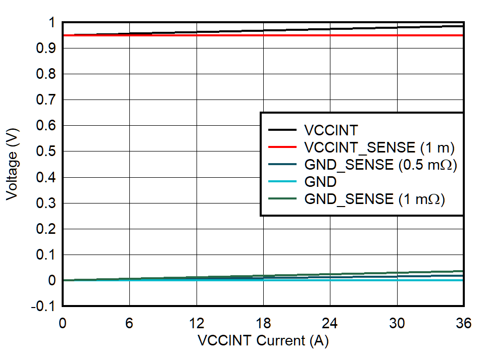
As the current supplied by the TPS7H4001-SP increases, the internal differential voltage across the XQRKU060 die might decrease, depending on the internal RGND_SENSE resistance. Figure 2-2 shows the relationship between VCCINT current and the different pin voltages for two different assumed values of internal package resistance. Both cases assume a nominal VCCINT voltage of 0.95 V.
 Figure 2-2 Voltages at the XQRKU060 Pins
as a Result of Sensing Pins
Figure 2-2 Voltages at the XQRKU060 Pins
as a Result of Sensing PinsThe first scenario in Figure 2-2 assumes the same resistance value of 1 mΩ for both RVCCINT_SENSE and RGND_SENSE. In this case, you can see how the VCCINT_SENSE voltage remains constant at 0.95 V (dotted red line), while the GND_SENSE voltage (dotted black line) increases as the VCCINT current increases.
GND signals and planes are typically the least resistive in ceramic packages given the large number of pins and planes used. Therefore, Figure 2-2 also shows an example where RVCCINT_SENSE = 1 mΩ but RGND_SENSE = 0.5 mΩ. In this particular case, the increase in the GND_SENSE voltage (dotted blue line) as the VCCINT current increases is much less than when RGND_SENSE = 1 mΩ. It is important to reemphasize that when using XPE, even this low RGND_SENSE value is compensated in the exact VCCINT value indicated.
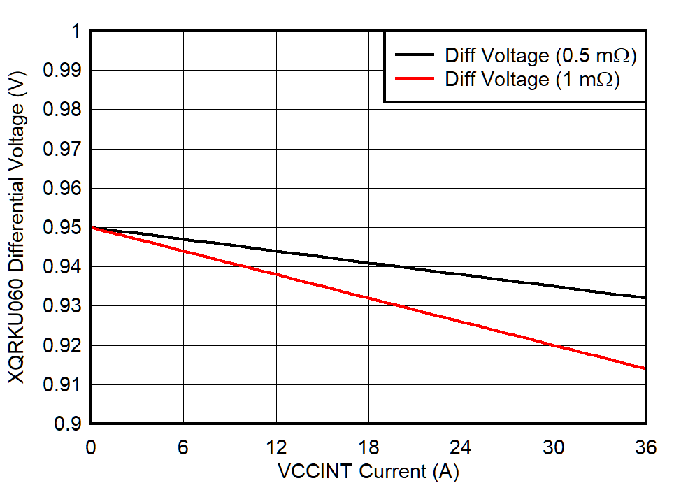
Figure 2-3 shows the impact of these two scenarios in the differential voltage across the XQRKU060 die. You can see that when RVCCINT_SENSE = RGND_SENSE = 1 mΩ, the differential voltage across the XQRKU060 die decreases to 0.914 V as the VCCINT current reaches 36 A. When RVCCINT_SENSE = 1 mΩ but RGND_SENSE = 0.5 mΩ, however, the differential voltage only decreases to 0.932 V as the VCCINT current reaches 36 A. While the 18-mV difference between these two scenarios might seem low, this translates to a 3.7% (VCCINTdiff = 0.914 V) vs. a 1.9% (VCCINTdiff = 0.932 V) DC-regulation tolerance (from 0.95-V nominal), which is significant in the context of VCCINT voltage tolerance requirements.
 Figure 2-3 Differential Voltage Across
the XQRKU060 for Two Different RGND_SENSE Values