SLVAF70 September 2021 TPS62130
3 Simulation and Experimental Results
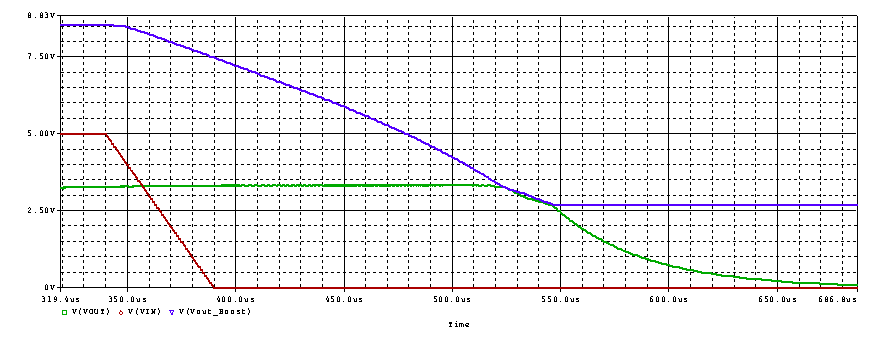
Figure 3-1 and Figure 3-2 show PSpice simulation results with the critical waveforms to verify the operation and performance of the proposed application method. The input and output voltages are 5 V and 3.3 V respectively, and the output current is 1 A for the simulation.
As Figure 3-1 shows, the output voltage of the boost converter is regulated even though there is no independent PWM controller. As VBOOST.OUT is determined by Equation 4, 8.3 V is calculated in this case. Since VBOOST.OUT is the input of the TPS62130, it is important to note that the input voltage of the TPS62130 goes up to a certain voltage level based on VIN and VOUT conditions.

Figure 3-1 PSpice Simulation Results in Steady State
Figure 3-2 shows VIN, VBOOST.OUT and VOUT. Though VIN is falling below 3.3 V, VBOOST.OUT is still high enough to regulate VOUT increasing hold-up time, and VOUT is being regulated until VBOOST.OUT reaches around 3.3 V, as shown in Figure 3-2.

Figure 3-2 PSpice Simulation Results (VIN, VBOOST.OUT, VOUT)
Figure 3-3 and Figure 3-4 show the related experimental waveforms (VIN: Ch1 in light blue with 1
V/div, VOUT: Ch2 in blue with 1 V/div) to see actual hold-up time with
1-A load condition, and the switching frequency is
1.25
MHz for this test. The TPS62130 evaluation module (TPS62130EVM-505) was used for
this measurement, and the hold-up time is 2.2 ms in this typical application
case.

Figure 3-3 Test Waveform With the Typical Application TPS62130 Method
A prototype schematic shown in Figure 2-2 was built and tested to verify the operation, and Figure 3-4 shows VIN and VOUT with the same 1-A load condition. As shown in Figure 3-4, the proposed application method has 7.2 ms hold-up time which is 5 ms longer compared to the typical application case of the TPS62130. Also, VOUT is still regulated to achieve a steady 3.3 V even though VIN goes down to around 1 V.

Figure 3-4 Test Waveform With the Proposed Application Method