SLVAF72 September 2021 TPS2661
4 HART Tests Done on TPS2661x
To test the performance of TPS2661x on HART protocol, the approach was to check the impact TPS2661x have on the loop current and the HART communication bits that were being transmitted. To figure the possibility of bit error being introduced by TPS2661x, multiple strategies were adopted in putting together the data set for the test. The data set covered the possibility of bit swap and bit flip errors being introduced by TPS2661x leakage currents. A sample data set is shown in Figure 4-1 and Figure 4-2. The reference data point will be HART transmission between HART transceivers without the Loop current protector. This data would be compared with the data received after adding the TPS2661x current loop protector in the communication loop. Tests were performed with different dc loop current settings.
Data set included the following:
- Single byte transmission
- Transmission of byte sequence in ascending order from 00 to FF
- Transmission of byte sequence in descending order from FF to 00
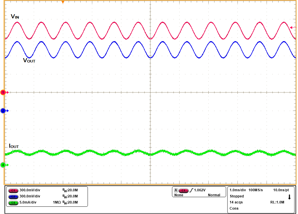
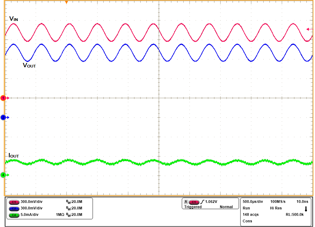
Results of the tests proved that, the low leakage current feature helped TPS2661x to provide the required protection without interfering with the analog dc loop current while allowing the HART communication. No bit flip or bit swap errors were also observed on HART communication with TPS2661x inserted in the communication loop. Figure 4-1 and Figure 4-2 show the HART communication through TPS2661x for a 0 and 1 transmission. Table 4-1 and Table 4-2 provide the HART data transmission results with TPS2661x device.
 Figure 4-1 1.2Khz HART Signal Through
TPS2661x
 Figure 4-2 2.2Khz HART Signal Through
TPS2661x
Figure 4-2 2.2Khz HART Signal Through
TPS2661x| Write Byte | Read Byte | Error Byte | Loop Current | Write Byte | Read Byte | Error Byte | Loop Current |
|---|---|---|---|---|---|---|---|
| Without TPS2661x | With TPS2661x | ||||||
| 0 | 0 | No Error | 4, 2.5, 7.5mA | 0 | 0 | No Error | 4, 2.5, 7.5mA |
| 1 | 1 | No Error | 4, 2.5, 7.5mA | 1 | 1 | No Error | 4, 2.5, 7.5mA |
| 2 | 2 | No Error | 4, 2.5, 7.5mA | 2 | 2 | No Error | 4, 2.5, 7.5mA |
| 3 | 3 | No Error | 4, 2.5, 7.5mA | 3 | 3 | No Error | 4, 2.5, 7.5mA |
| 4 | 4 | No Error | 4, 2.5, 7.5mA | 4 | 4 | No Error | 4, 2.5, 7.5mA |
| 5 | 5 | No Error | 4, 2.5, 7.5mA | 5 | 5 | No Error | 4, 2.5, 7.5mA |
| 6 | 6 | No Error | 4, 2.5, 7.5mA | 6 | 6 | No Error | 4, 2.5, 7.5mA |
| 7 | 7 | No Error | 4, 2.5, 7.5mA | 7 | 7 | No Error | 4, 2.5, 7.5mA |
| 8 | 8 | No Error | 4, 2.5, 7.5mA | 8 | 8 | No Error | 4, 2.5, 7.5mA |
| 9 | 9 | No Error | 4, 2.5, 7.5mA | 9 | 9 | No Error | 4, 2.5, 7.5mA |
| A | A | No Error | 4, 2.5, 7.5mA | A | A | No Error | 4, 2.5, 7.5mA |
| B | B | No Error | 4, 2.5, 7.5mA | B | B | No Error | 4, 2.5, 7.5mA |
| Write Byte | Read Byte | Error Byte | Loop Current | Write Byte | Read Byte | Error Byte | Loop Current |
|---|---|---|---|---|---|---|---|
| Without TPS2661x | With TPS2661x | ||||||
| FF | FF | No Error | 4, 2.5, 7.5mA | FF | FF | No Error | 4, 2.5, 7.5mA |
| FE | FE | No Error | 4, 2.5, 7.5mA | FE | FE | No Error | 4, 2.5, 7.5mA |
| FD | FD | No Error | 4, 2.5, 7.5mA | FD | FD | No Error | 4, 2.5, 7.5mA |
| FC | FC | No Error | 4, 2.5, 7.5mA | FC | FC | No Error | 4, 2.5, 7.5mA |
| FB | FB | No Error | 4, 2.5, 7.5mA | FB | FB | No Error | 4, 2.5, 7.5mA |
| FA | FA | No Error | 4, 2.5, 7.5mA | FA | FA | No Error | 4, 2.5, 7.5mA |
| F9 | F9 | No Error | 4, 2.5, 7.5mA | F9 | F9 | No Error | 4, 2.5, 7.5mA |
| F8 | F8 | No Error | 4, 2.5, 7.5mA | F8 | F8 | No Error | 4, 2.5, 7.5mA |
| F7 | F7 | No Error | 4, 2.5, 7.5mA | F7 | F7 | No Error | 4, 2.5, 7.5mA |
| F6 | F6 | No Error | 4, 2.5, 7.5mA | F6 | F6 | No Error | 4, 2.5, 7.5mA |
| F5 | F5 | No Error | 4, 2.5, 7.5mA | F5 | F5 | No Error | 4, 2.5, 7.5mA |
| F4 | F4 | No Error | 4, 2.5, 7.5mA | F4 | F4 | No Error | 4, 2.5, 7.5mA |
| F3 | F3 | No Error | 4, 2.5, 7.5mA | F3 | F3 | No Error | 4, 2.5, 7.5mA |