SLVAFC5 March 2022 TPS629210 , TPS629210-Q1
6 Typical Performance and Waveforms
The application circuit shown in Figure 6-1 is used to generate the data for typical performance. L1 is a 2.2 µH inductor from Coilcraft, whereas a 2.2 µH XGL3530-222MEC is used. The output capacitors used 3x22 µF, 10 V, 0603, X5R ceramic capacitor. The input capacitor used 10 μF, 25V, 0603, X5R. Unless otherwise specified, VIN = 12 V and VOUT = –3.3 V, IOUT=0 A to 0.76 A, 2.5 MHz, Auto PFM/PWM, internal feedback (VSET).
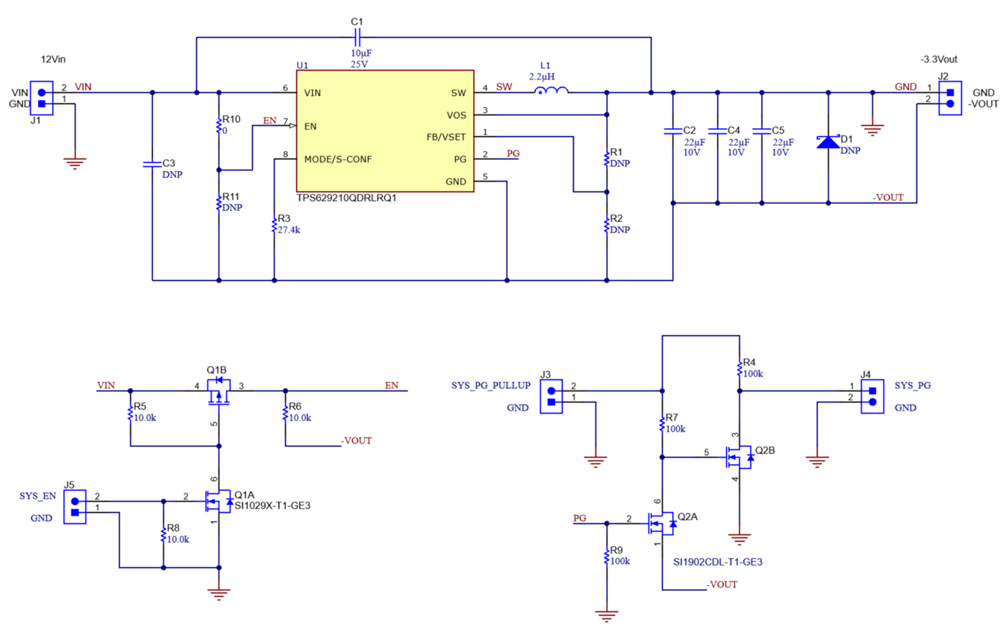 Figure 6-1 Schematic
of Tested Circuit
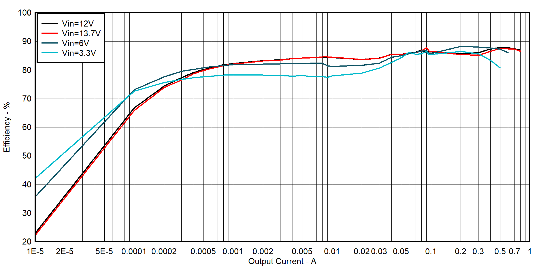 Figure 6-2
Efficiency with VOUT = –3.3 V
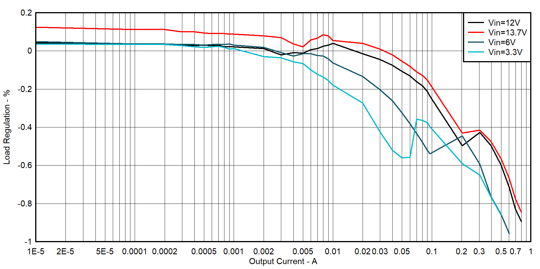 Figure 6-3 Load
Regulation with VOUT = –3.3 V
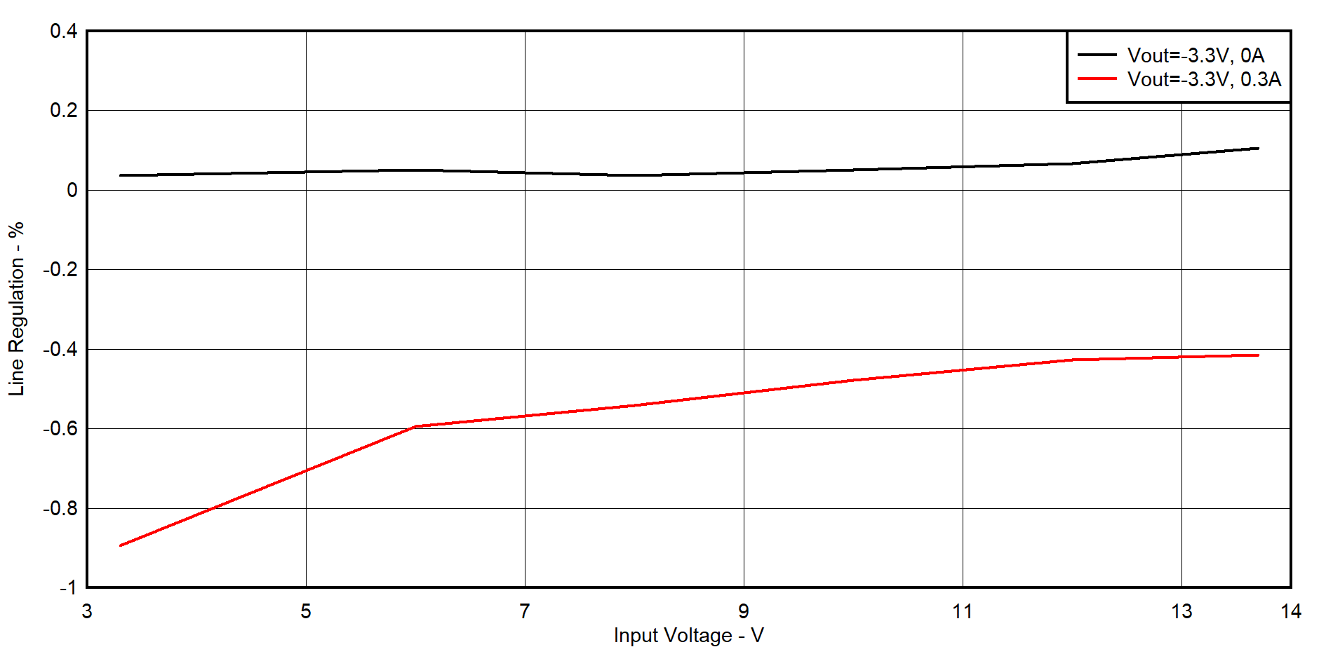 Figure 6-4 Line
Regulation with VOUT = –3.3 V , IOUT = 0 A and 0.3 A
 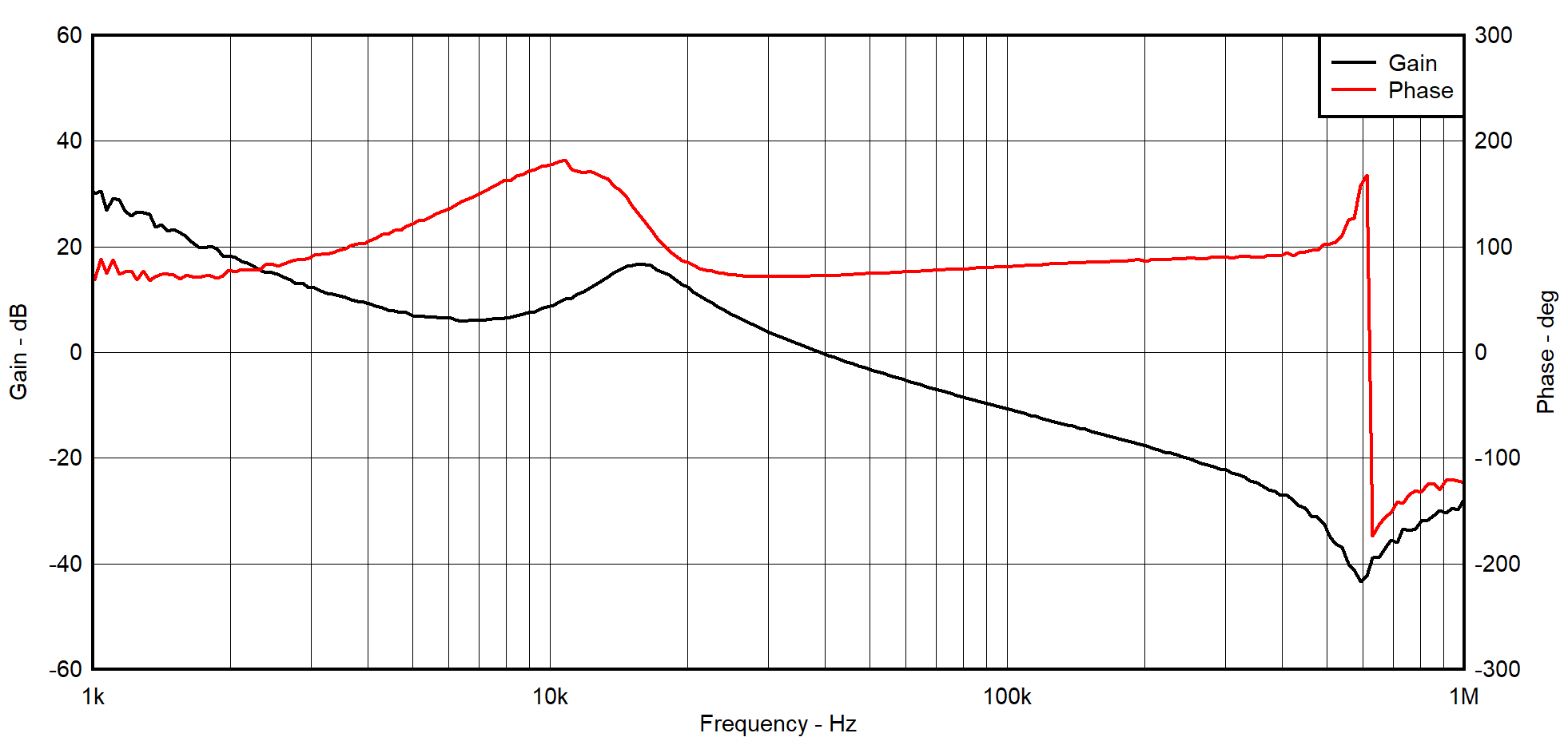 Figure 6-5 Loop
Response with VIN =12 V, VOUT = –3.3 V, IOUT =
0.5A
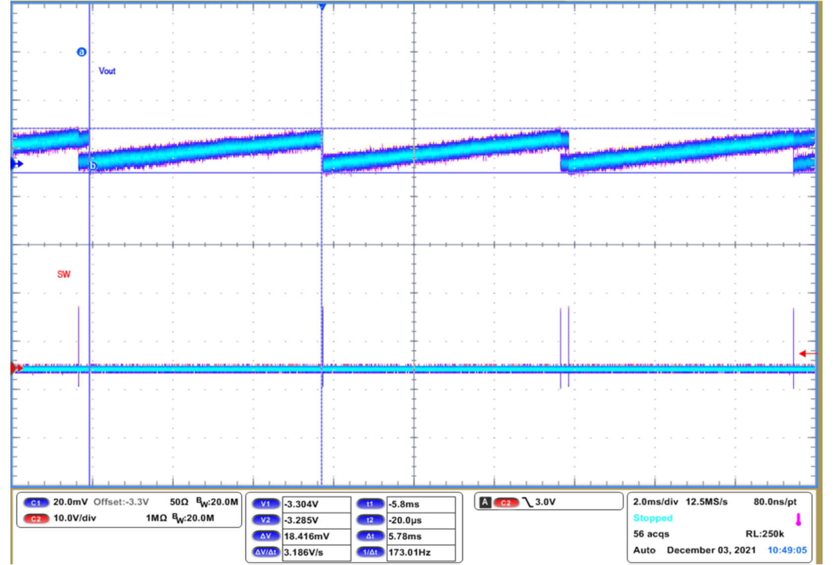 Figure 6-6 Output
Voltage Ripple with VIN = 12 V, VOUT = -3.3 V,
IOUT = 0 A
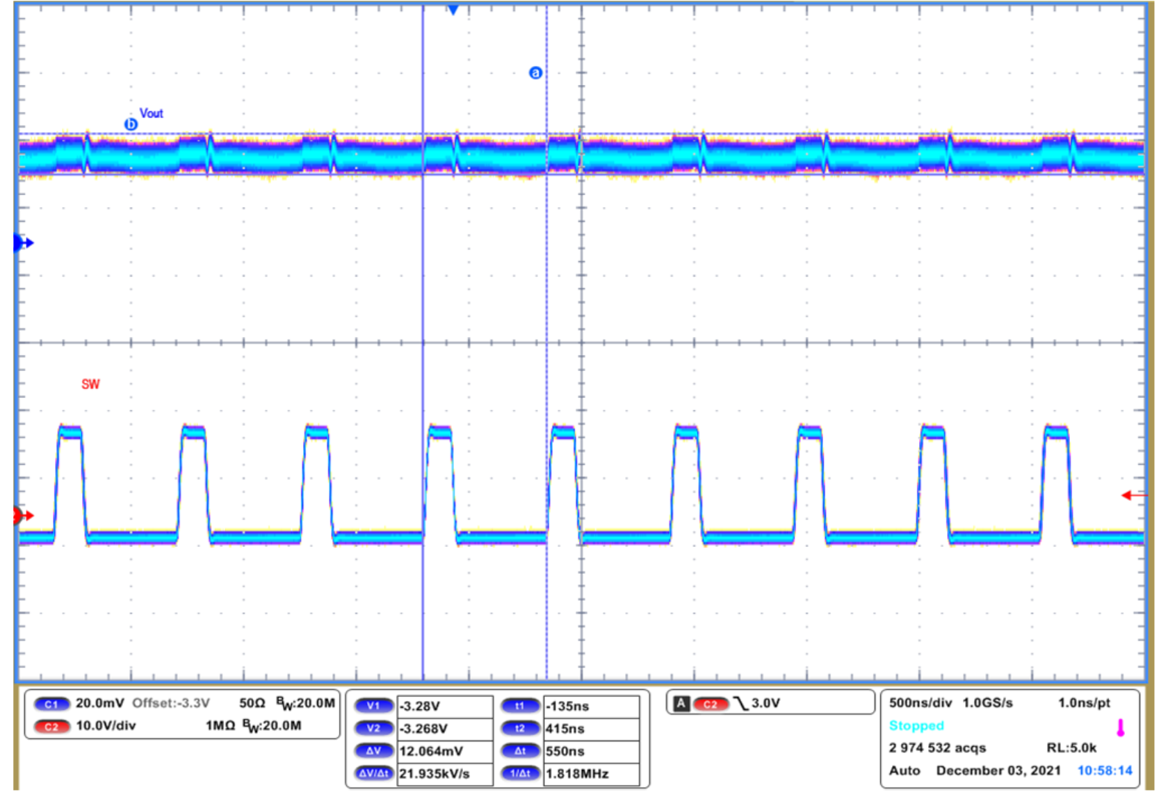 Figure 6-7 Output
Voltage Ripple with VIN = 12 V, VOUT = -3.3 V,
IOUT = 0.5 A
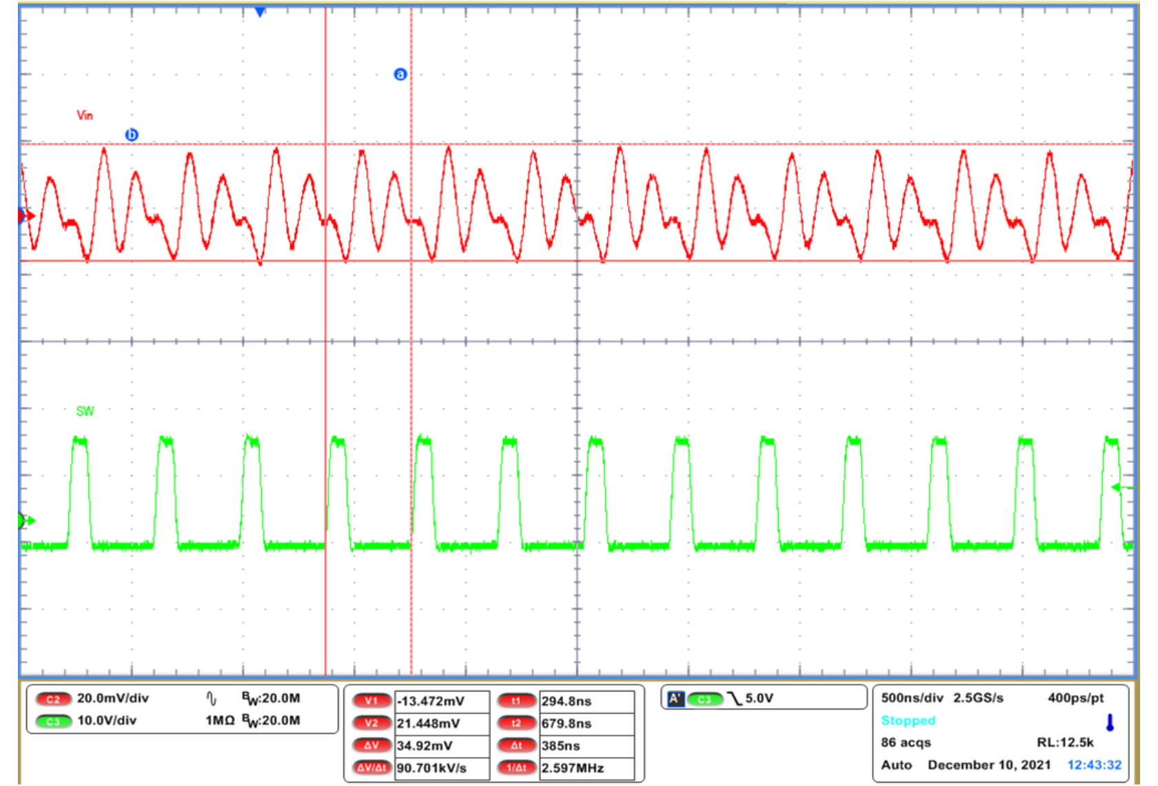 Figure 6-8 Input
Voltage Ripple with VIN = 12 V , VOUT = -3.3 V,
IOUT = 0.5 A
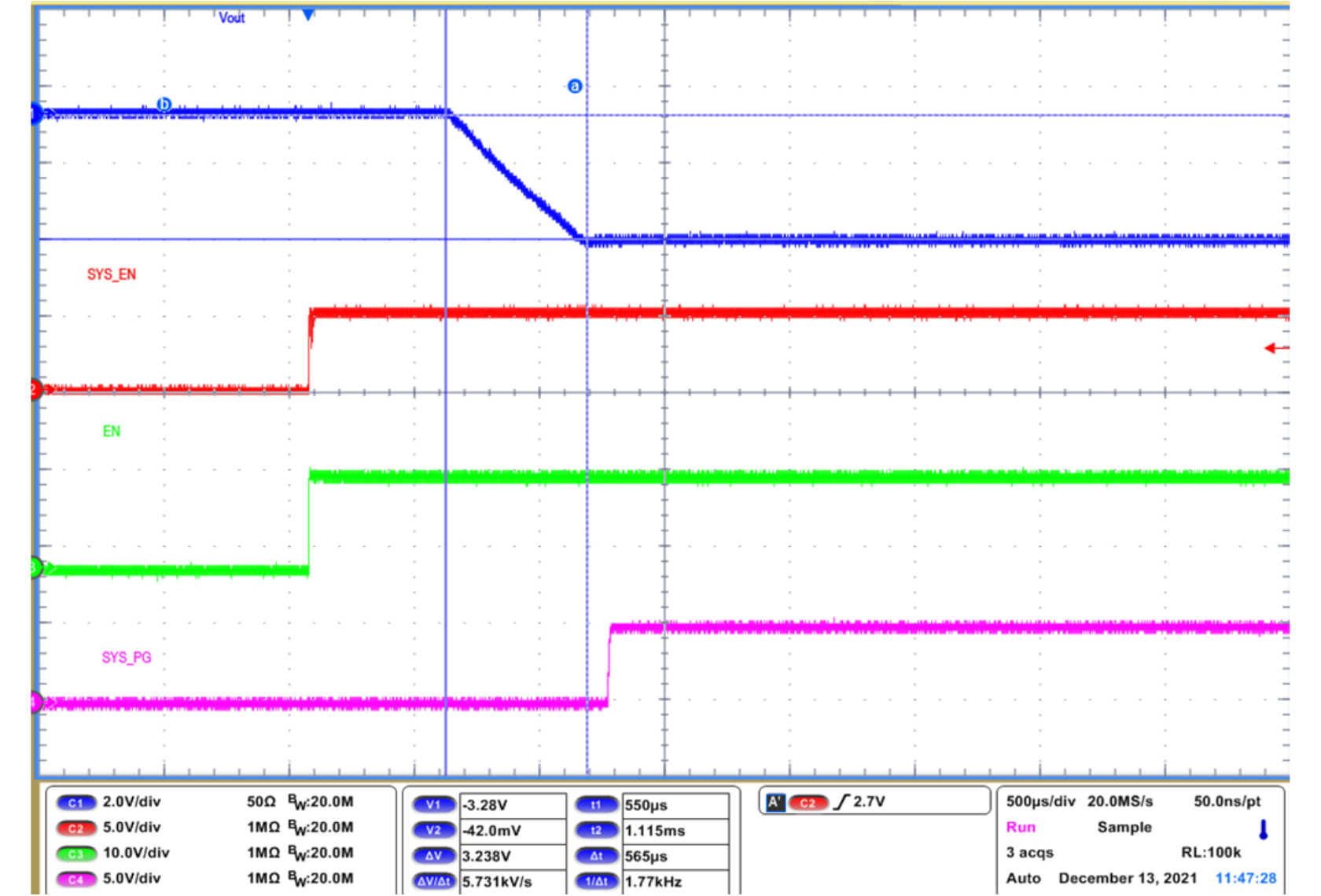 Figure 6-9 Enable Start up with
VIN = 12 V, VOUT = -3.3 V, IOUT = 0.5
A
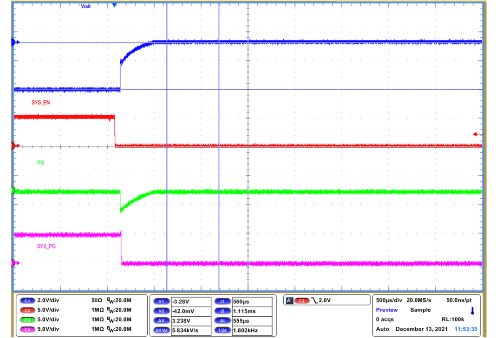 Figure 6-10 Enable shutdown with
VIN= 12 V, VOUT = -3.3 V, IOUT = 0.5
A
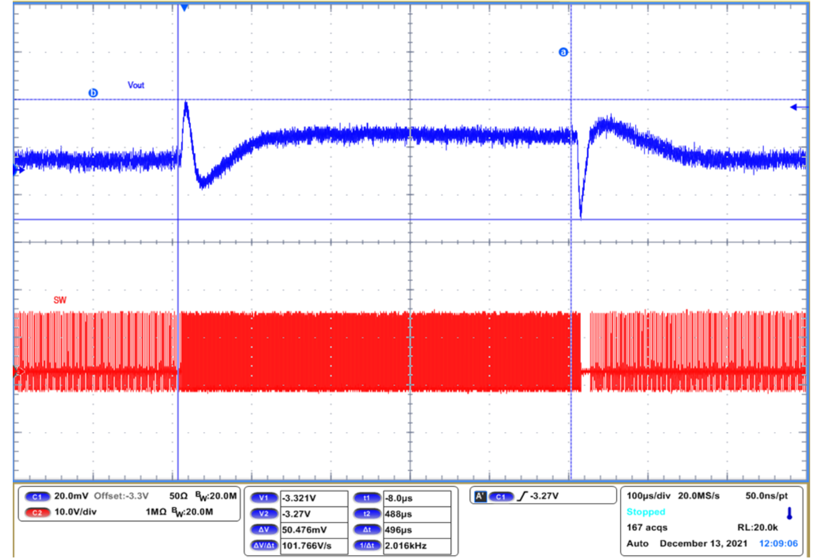 Figure 6-11 Load Transient with
VIN = 12 V, VOUT = -3.3 V, IOUT = 0.1 A to
0.6 A, Slew rate 1A/μs
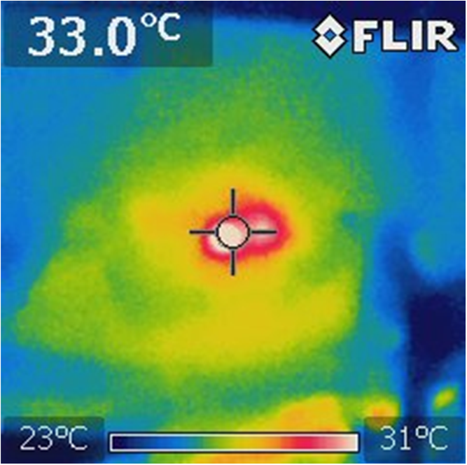 Figure 6-12 Thermal Performance with
VIN = 12 V, VOUT =-3.3 V, IOUT = 0.76 A, 10
mimutes soaking