SLVAFE7 September 2022 LM51551
2.3 Voltage Control by External Signal
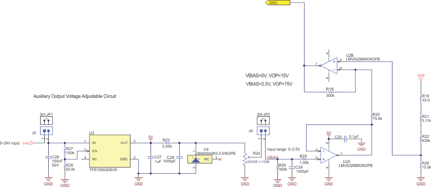
Adjustable outputs can meet the requirement from different customers and make it easy to power the transmitter since the design may need several voltage rails. In this design, a signal (0 V to 2.5 V) from FPGA is used to control the output voltage by comparing the feedback voltage captured from the positive output. The output of the op amp is connected to the FB pin of the LM51551 device to regulate the VOUT.
 Figure 2-4 Output Voltage Control by
External Signal
Figure 2-4 Output Voltage Control by
External SignalFigure 2-5 shows the diagram of the voltage control circuit. To select the proper value of R18, R19, R20, R21, R22, and R26, see the following equations.
where
- Vref is the reference voltage of the FB pin in LM51551
- Vctrl is the desired control voltage range of the customers
- kFB, ka, and kb are the ratio of the resistors which helps to define the value
For example, the following equations show that if kFB = 1.5 , desired control voltage is 0 V to 2.5 V and the output voltage is 15 V to 75 V: