SLVAFF7B December 2022 – November 2024 TPS25762-Q1 , TPS25763-Q1 , TPS25772-Q1
4.3.2 Burst Mode Patch Download Process
The following is the flow diagram detailing the process for burst mode download.
 Figure 4-5 Flow Diagram of Patch Bundle Update –
Burst Mode Download
Figure 4-5 Flow Diagram of Patch Bundle Update –
Burst Mode DownloadFigure 4-5 shows the process for burst mode download. After the host confirms that the device has entered PTCH mode, the host shall implement the sequence below to download the patch bundle:
- The host initializes the firmware in
preparation for a PBMx load sequence and what the patch bundle contains by writing
6 bytes of data to the DATAx (0x09 if using I2C1 or 0x11 if using I2C2) register:
- 0x06 is first transmitted to tell the PD controller a 6-byte payload is written.
- Bytes 0 to 3 are the patch bundle size. In Figure 4-6, the patch bundle size is 0x3500 or 13568 bytes. Byte 4 is the DATAx.SlaveAddress you want to assign for data transmission. 0x00 or the device's I2C slave addresses (0x22/0x26 or 0x23/0x27) of the PD controller are not valid. Figure 4-6 shows a random address, 0x35, was selected and used.
- Byte 5 is the burst mode timeout value (LSB of 100ms). A non-zero value must be used and is recommended to always use 0x32, that gives you a 5 second window to complete the burst mode patch update.
 Figure 4-6 Patch Burst Mode
Initialization
 - The host shall start the burst mode patch
download process by sending the 4CC ASCII PBMs task command to the CMDx (0x08 if
using I2C1 or 0x10 if using I2C2) register. 0x04 is first transmitted to tell the PD
controller that a total of 4 bytes will be written.
 Figure 4-7 PBMs Task Command
 - Read and poll the CMDx register until
Byte 1 is 0x00, indicating that the task processing is finished.
 Figure 4-8 CMDx Output - Task Processing
Completed
 - Read and poll
the DATAx register until Byte 1 is 0x00, indicating that the patch initialization from
step 1 was successful.
 Figure 4-9 DATAx Output - Successful Patch
Initialization
 - Transmit patch bundle data to the
DATAx.SlaveAddress configured in step 1 in packets of 256 byte. The patch bundle can be
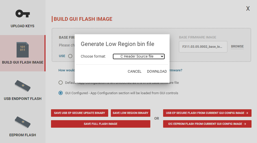
generated as a C style array using the TPS257XX-Q1-GUI (available from v1.2.0). From the BUILD GUI FLASH IMAGE
menu, select SAVE LOW REGION BINARY. Then choose the C Header Source File as the format
and click SAVE. This file will also include the patch bundle size.
 Figure 4-10 Generating Patch Bundle as C
Array
 - After the patch
bundle data is successfully written, wait 500us and write the PBMc task to the CMDx
register to complete the patch loading sequence. Ensure you are back to writing to the
original I2C slave address of the PD controller from this step.
 Figure 4-11 PBMc Task Command
 - Read and poll the CMDx register until Byte 1 is 0x00, indicating that the task processing is finished.
- Read and poll the DATAx register until Byte 1 is 0x00, indicating that the device patch bundle download was successful. The I2C Interrupt, or GPIO9, will be released roughly 110 ms after.
- Write the PBMe task to the CMDx
register to end the patch loading sequence and enter ‘APP’ mode (optional).
 Figure 4-12 PBMe Task Command
 - Read the MODE register to check if the device is in APP mode which indicates that the PD controller received all patch and application configuration data and is fully functioning in the application firmware.