SLVAFI8 February 2023 TLC6C5748-Q1
- Abstract
- Trademarks
- 1Introduction
-
2Design Considerations for Low EMI
- 2.1 Design Considerations Overview
- 2.2
Considerations in Detail
- 2.2.1 Top-Level Architecture
- 2.2.2
High Frequency Signals
- 2.2.2.1 Original Setup
- 2.2.2.2 3.3 V I/O Voltage Instead of 5 V
- 2.2.2.3 Use Independent OSC for GSCLK With Spread Spectrum
- 2.2.2.4 Without Using Buffer on GSCLK
- 2.2.2.5 Using Snubber on GSCLK
- 2.2.2.6 Lower the Signal Frequency
- 2.2.2.7 Placement and PCB layout
- 2.2.2.8 ESD Enhancement
- 2.2.2.9 Demo and Test Results
- 2.2.2.10 Bench Test Results
- 3Summary
- 4References
2.2.2.10 Bench Test Results
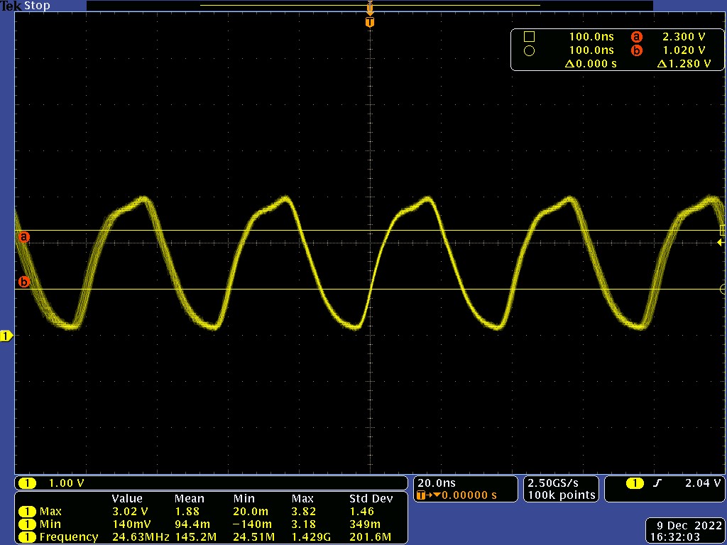
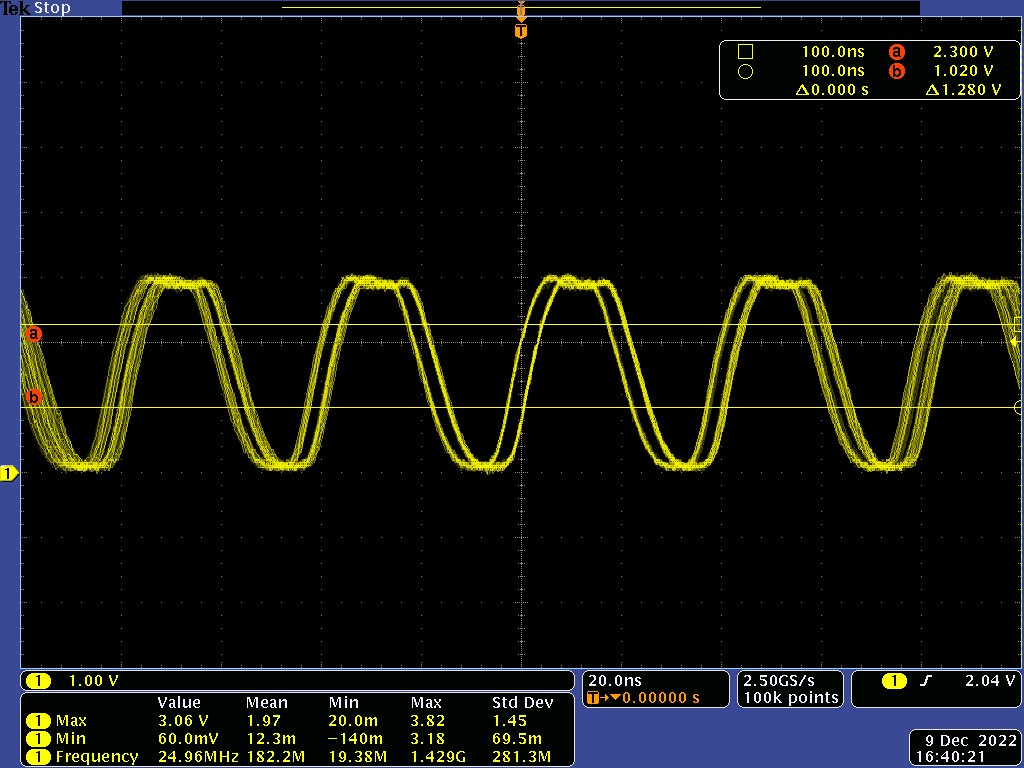
After adding countermeasures, checking if the signal integrity is essential, especially GSCLK. Sometimes, GSCLK waveform was affected when adding snubber. Per the data sheet, it should be checked whether GSCLK meet the chip criteria high/low pulse larger than 10us. For the TLC6C5748-Q1 structure, checking first TLC6C5748-Q1 and last TLC6C5748-Q1 GSCLK pin to confirm whether meeting the data sheet.
 Figure 2-13 First TLC6C5748-Q1 GSCLK
Waveform
 Figure 2-14 Last TLC6C5748-Q1 GSCLK
Waveform