SLVAFM7 June 2024 TLC6983
3.1.2 Upside Ghosting
Actually, the root cause analysis of upside ghosting is similar to what has been discussed in the downside ghosting session. The main cause of upside ghosting is the buildup charge in the parasitic capacitance on SWn when transitioning between scan lines, the parasitic capacitance is charged through the LED causing this to light up when this must not be. Figure 3-9, Figure 3-10 and Figure 3-11 describe the root cause analysis of upside ghosting.
So, in P1 operation, when only wants to light up LED02, the driver turns ON SW0. And at this moment, the yellow parasitic capacitor on Scan Line 0 is discharged to 0, through these current paths in red dotted line.
During P1 operation, SW0 is ON, LED02 lights up.
 Figure 3-9 Upside ghosting - P1 Operation
Next, in P2 operation, when only wants to light up LED11, the driver turns on SW1 and the yellow parasitic capacitor on Scan Line 1 is discharged to 0, through these current paths in red dotted line. However, at this moment, the yellow parasitic capacitor on Scan Line 0 is also charged, through the current path in blue dotted line. So, LED01 is slightly light up even SCAN line 0 is closed. Because the parasitic capacitor on SCAN line 0 has been discharged previously, and LED01 is light up through the current path in blue dotted line. So, LED01 is calling upside ghosting.
During P2 operation, SW1 is ON, LED11 lights up, LED01 slightly lights up.
 Figure 3-10 Upside ghosting - P2 Operation
Similarly, in P3 operation, when only wanting to light up LED20, we can see that LED10 is slightly lit up and LED00 is even so slightly lit up, through the current paths in blue and orange dotted line, respectively. The reason is the same as previously due to the scan line parasitic capacitors.
The reason that LED10 and LED00 have different brightness is because the corresponding scan line parasitic capacitors accumulate different charges before the LED being faulty lighted up (different quantities of charge flow through the LED to charge the corresponding scan line parasitic capacitor).
During P3 operation, SW2 is ON, LED20 lights up, LED10 slightly lights up, LED00 ever so slightly lights up.
 Figure 3-11 Upside ghosting - P3 Operation
So, how to solve this issue? The upside ghosting is because of discharges on SCAN line parasitic capacitors. So, if we can stop or weaken the discharge process, then we can solve this issue.
As shown in Figure 3-12, TLC698x uses scan line clamp circuits to pull up the line voltage to a high value (Vclamp) during the line switch time to maintain no current flow to the previous scan line, thus eliminating upside ghosting.
 Figure 3-12 Upside Ghost Effect Elimination by SW Line Clamp Circuit
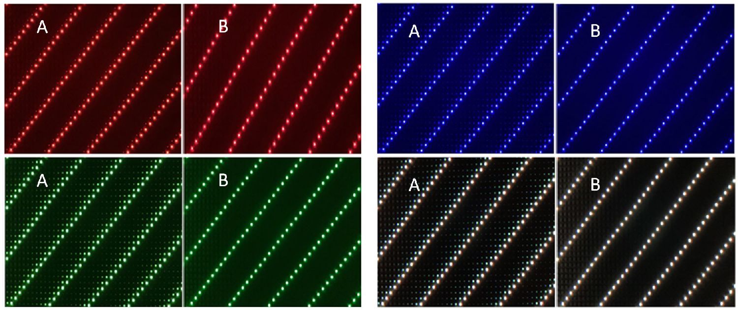
Figure 3-13 shows the comparison demo with or without upside ghosting. We can see that the clamp circuit works very well. With this being enabled, we do not see ghosting anymore.
 Figure 3-13 Comparison Demo With or Without Upside Ghosting