SLVAFU0 April 2024 TPS61377
2 Analysis of Dual Polarity Voltage Rails Design With Boost Converter
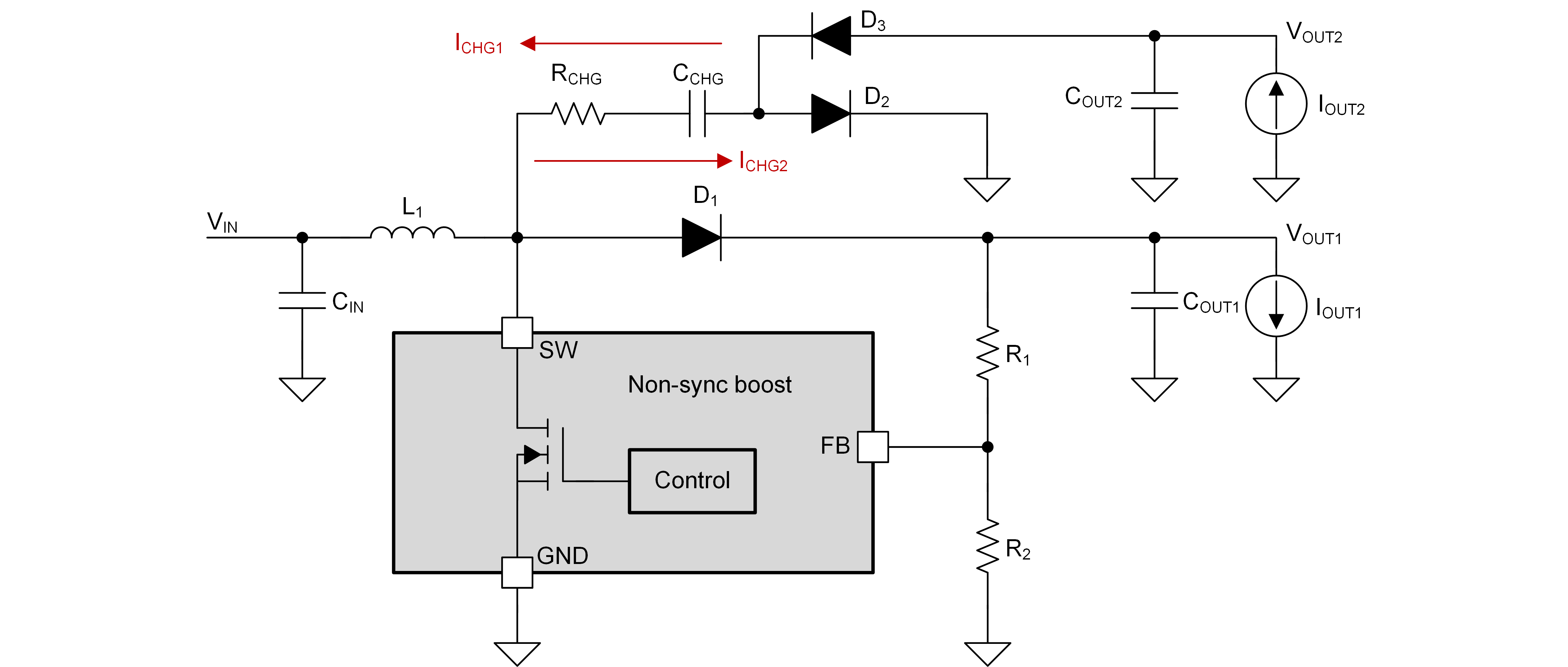
Figure 2-1 shows the typical circuit of dual polarity voltage rails design with asynchronous boost converter. The image uses the RCHG, CCHG, D2 and D3 to achieve the negative voltage rail.
 Figure 2-1 Typical Circuit of Dual
Polarity Voltage Rails Design With Asynchronous Boost Converter