SLVAFU0 April 2024 TPS61377
4.1 Simulation Results
Simulation uses the Table 4-1 test parameters to analyze the function of R3 in Figure 4-1.
Table 4-1 Test Parameters
| Test parameters | |
|---|---|
| Input voltage | 12V |
| Output voltage | ± 19V |
| Output load | ± 500mA |
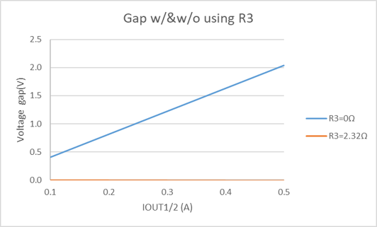
Table 4-2 shows the gap between with using R3 and without using R3. R3 can effectively eliminate the DC offset using the architecture.
Table 4-2 Gap With and Without Using
R3
| IOUT1/2 (A) | R3=2.32ohm, Gap(V) | R3 = 0ohm, Gap(V) |
|---|---|---|
| 0 | 0.0000 | 0.0000 |
| 0.1 | -0.0005 | 0.41 |
| 0.2 | -0.0010 | 0.82 |
| 0.3 | -0.0015 | 1.22 |
| 0.4 | -0.0021 | 1.63 |
| 0.5 | -0.0024 | 2.04 |
 Figure 4-1 Gap With and Without Using
R3