SLVAFU0 April 2024 TPS61377
4.2 Demo Board Example
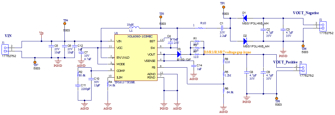
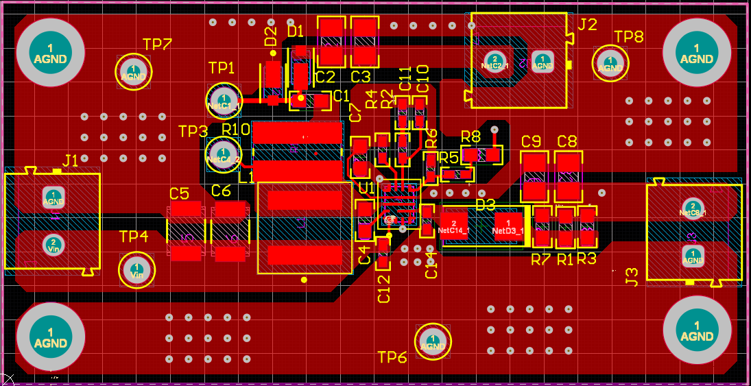
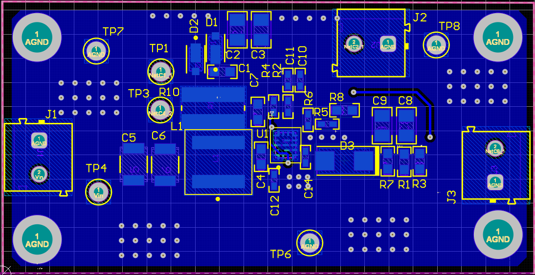
Figure 4-2, Figure 4-3, and Figure 4-4 demonstrate a schematic and two-layered layout example using TPS61377 to achieve Table 4-1 requirements. To minimize the output power loop, the recommendation is to add 1µF capacitor on VOUT pin to GND like C14 showing in the schematic.
 Figure 4-2 TPS61377 Schematic
 Figure 4-3 TPS61377 Layout (Top)
 Figure 4-4 TPS61377 Layout
(Bottom)