SLVAFV4 July 2024 TLV62085
Overview
This document contains the pin failure mode analysis (pin FMA) information for the TLV62085.
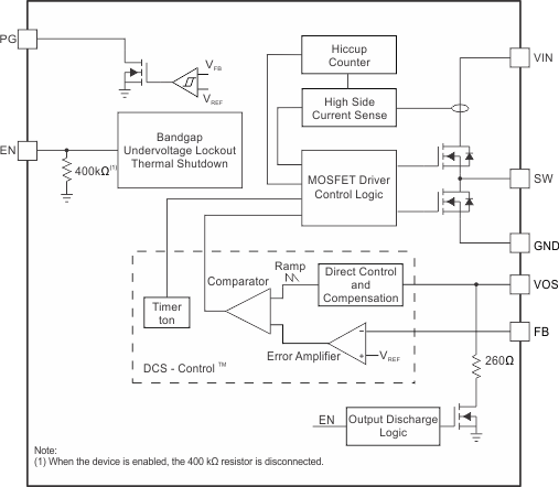
Figure 1 is showing the device functional-block diagram for reference.
 Figure 1 Functional Block
Diagram
Figure 1 Functional Block
DiagramPin Failure Mode Analysis (Pin FMA)
This section provides a failure mode analysis (FMA) for the pins of the TLV62085. The failure modes covered in this document include the typical pin-by-pin failure scenarios:
- Pin short-circuited to ground (see Table 2)
- Pin open-circuited (see Table 3)
- Pin short-circuited to an adjacent pin (see Table 4)
- Pin short-circuited to VIN (see Table 5)
Table 2 through Table 5 also indicate how these pin conditions can affect the device as per the failure effects classification in Table 1.
| Class | Failure Effects |
|---|---|
| A | Potential device damage that affects functionality. |
| B | No device damage, but loss of functionality. |
| C | No device damage, but performance degradation. |
| D | No device damage, no impact to functionality or performance. |
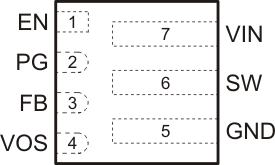
Figure 2 is showing the TLV62085 pin diagram. For a detailed description of the device pins, see the TLV62085 High Efficiency 3-A Step-Down Converter in 2-mm × 2-mm VSON Package Data Sheet.
 Figure 2 Pin Diagram
The following are the assumptions of use and the device configuration assumed for the pin FMA in this section:
- The device is operating in the typical application, see the TLV62085 High Efficiency 3-A Step-Down Converter in 2-mm × 2-mm VSON Package Data Sheet.
| Pin Name | Pin No. | Description of Potential Failure Effect(s) | Failure Effect Class |
|---|---|---|---|
| EN | 1 | Device is not enabled | B |
| PG | 2 | Loss of PG functionality | B |
| FB | 3 | Output voltage not regulated; device enters 100% duty cycle or current limit operations | B |
| VOS | 4 | Output voltage not regulated; device enters 100% duty cycle or current limit operations | B |
| GND | 5 | Intended functionality | D |
| SW | 6 | Device not functional | A |
| VIN | 7 | Devices does not power up | A |
| Pin Name | Pin No. | Description of Potential Failure Effect(s) | Failure Effect Class |
|---|---|---|---|
| EN | 1 | Internal pull-down keeps this pin low; device disabled | B |
| PG | 2 | Loss of PG functionality | B |
| FB | 3 | Undetermined behavior of pin FB; open loop operation; output voltage not regulated. | B |
| VOS | 4 | Reduced transient performance. No output discharge available. Potentially reduced current limit. | B |
| GND | 5 | Incorrect device functionality | B |
| SW | 6 | Device not functional; open loop operations; no output voltage | B |
| VIN | 7 | Devices does not power up | B |
| Pin Name | Pin No. | Shorted to | Pin No. | Description of Potential Failure Effect(s) | Failure Effect Class |
|---|---|---|---|---|---|
| EN | 1 | PG | 2 | Undetermined device operation; device may or may not power up | B |
| PG | 2 | FB | 3 | Incorrect device functionality due to disturbed feedback path | B |
| PG | 2 | SW | 6 | Potential device damaged for the internal open-drain pulldown; loss of PG indication | A |
| FB | 3 | VOS | 4 | Device regulates to 0.8V output voltage only | B |
| FB | 3 | SW | 6 | Incorrect device functionality due to disturbed feedback path | B |
| GND | 5 | FB | 3 | Output voltage not regulated; device enters 100% duty cycle or current limit operations | B |
| GND | 5 | VOS | 4 | Output voltage not regulated; device enters 100% duty cycle or current limit operations | B |
| GND | 5 | SW | 6 | Device not functional | A |
| VIN | 7 | EN | 1 | Device enabled for VIN ≥ V_UVLO and VIN ≥ VIN_min | B |
| VIN | 7 | SW | 6 | Device not functional | A |
| Pin Name | Pin No. | Description of Potential Failure Effect(s) | Failure Effect Class |
|---|---|---|---|
| EN | 1 | Device enabled for VIN ≥ V_UVLO and VIN ≥ VIN_min | B |
| PG | 2 | Potential device damaged for the internal open-drain pulldown | A |
| FB | 3 | Output voltage not regulated; output voltage is regulated to 0V | B |
| VOS | 4 | Output voltage not regulated | A |
| GND | 5 | Device does not power up | A |
| SW | 6 | Device not functional | A |
| VIN | 7 | Intended functionality | D |