SLVAFV8 July 2024 TPS25751
2 ADCINX Setting
Set the appropriate ADCINX value is the first way to use I2Ct normally. The recommendation is to refer to Table 2-1 from TPS25751 data sheet. For the application, ADCINX uses the EC and so AlwaysEnableSink or NegotiateHighVoltage is recommended for dead battery configuration. Note, that if there is no EEPROM that cannot load patch file, use the SafeMode. Then, set the I2C ADDRESS INDEX that does not conflict the other I2C address on I2C bus. Here, ADCINX set #1 for the example.
After defining the ADCINX decode value, the ADCINX can get unique I2C address of TPS25751 from Table 2-2. For the setting, TPS25751 unique I2C address is 0x20.
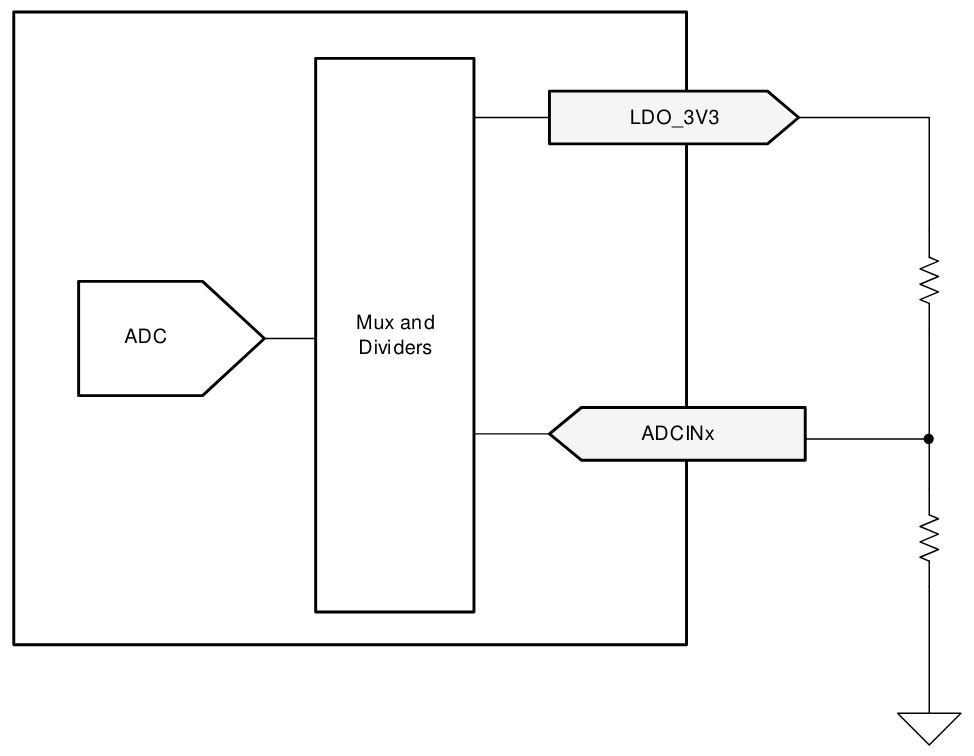
Table 2-3 show the recommended resistance for setting the desired ADCINX decoded value. The ADCINX pins must be externally dire to the LDO_3V3 pin via a resistive divider as shown in Figure 2-1.
| ADCIN1 Decoded Value | ADCIN2 Decoded Value | I2C Address Index | Dead Battery Configuration |
|---|---|---|---|
| 7 | 5 | #1 | AlwaysEnableSink: The device always enables the sink path regardless of the amount of current the attached source is offering. USB PD is disabled until configuration is loaded. This configuration is used with an external embedded controller. The embedded controller manages the battery charger in the system when present. |
| 5 | 5 | #2 | |
| 2 | 0 | #3 | |
| 1 | 7 | #4 | |
| 7 | 3 | #1 | Negotiate High Voltage: The device always enables the sink path during the initial implicit contract regardless of the amount of current the attached source is offering. The PD controller enters the APP' mode, enable USB PD PHY and negotiate a contract for the highest power contract that is offered up to 20V. The configuration cannot be used when a patch is loaded from EEPROM. This option is not recommended for systems that can boot from 5V. This configuration is not valid to use with any supported battery chargers. |
| 3 | 3 | #2 | |
| 4 | 0 | #3 | |
| 3 | 7 | #4 | |
| 7 | 0 | #1 | SafeMode: The device does not enable the sink path. USB PD is disabled until configuration is loaded. Note that the configuration can put the device into a source-only mode. This is recommended when the application loads the patch from EEPROM. This configuration is recommended when the PD controller manages the battery charger when present. |
| 0 | 0 | #2 | |
| 6 | 0 | #3 | |
| 5 | 7 | #4 |
| I2C Address Index (Decoded From ADCIN1 and ADCIN2) | BIT 7 |
BIT 6 |
BIT 5 |
BIT 4 |
BIT 3 |
BIT 2 |
BIT 1 |
BIT 0 |
Available During Boot |
|---|---|---|---|---|---|---|---|---|---|
| #1 | 0 | 1 | 0 | 0 | 0 | 0 | 0 | R/W | YES |
| #2 | 0 | 1 | 0 | 0 | 0 | 0 | 1 | R/W | YES |
| #3 | 0 | 1 | 0 | 0 | 0 | 1 | 0 | R/W | YES |
| #4 | 0 | 1 | 0 | 0 | 0 | 1 | 1 | R/W | YES |
| DIV = Rdown/(Rup and Rdown) | Without Using RUP or RDOWN | ADCINX Decode Value | ||
|---|---|---|---|---|
| MIN | Target | MAX | ||
| 0 | 0.0114 | 0.0228 | Tie to GND | 0 |
| 0.0229 | 0.0475 | 0.0722 | N/A | 1 |
| 0.0723 | 0.1074 | 0.1425 | N/A | 2 |
| 0.1425 | 0.1899 | 0.2372 | N/A | 3 |
| 0.2373 | 0.3022 | 0.3671 | N/A | 4 |
| 0.3672 | 0.5368 | 0.7064 | Tie to LDO_1V5 | 5 |
| 0.7065 | 0.8062 | 0.9060 | N/A | 6 |
| 0.9061 | 0.9530 | 1.0 | Tie to LDO_3V3 | 7 |
 Figure 2-1 ADCINX Resistor
Divider