SLVK172 June 2024 TPS7H3014-SP
- 1
- TPS7H3014-SP Single-Event Effects (SEE)
- Trademarks
- 1 Introduction
- 2 Single-Event Effects (SEE)
- 3 Device and Test Board Information
- 4 Irradiation Facility and Setup
- 5 Depth, Range, and LETEFF Calculation
- 6 Test Setup and Procedures
- 7 Destructive Single-Event Effects (DSEE)
- 8 Single-Event Transients (SET)
- 9 Event Rate Calculations
- 10Summary
- A References
3 Device and Test Board Information
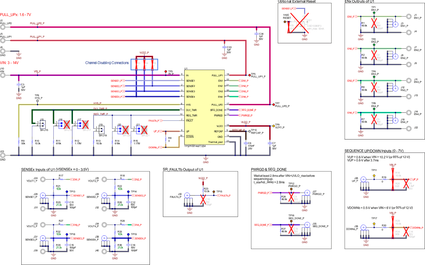
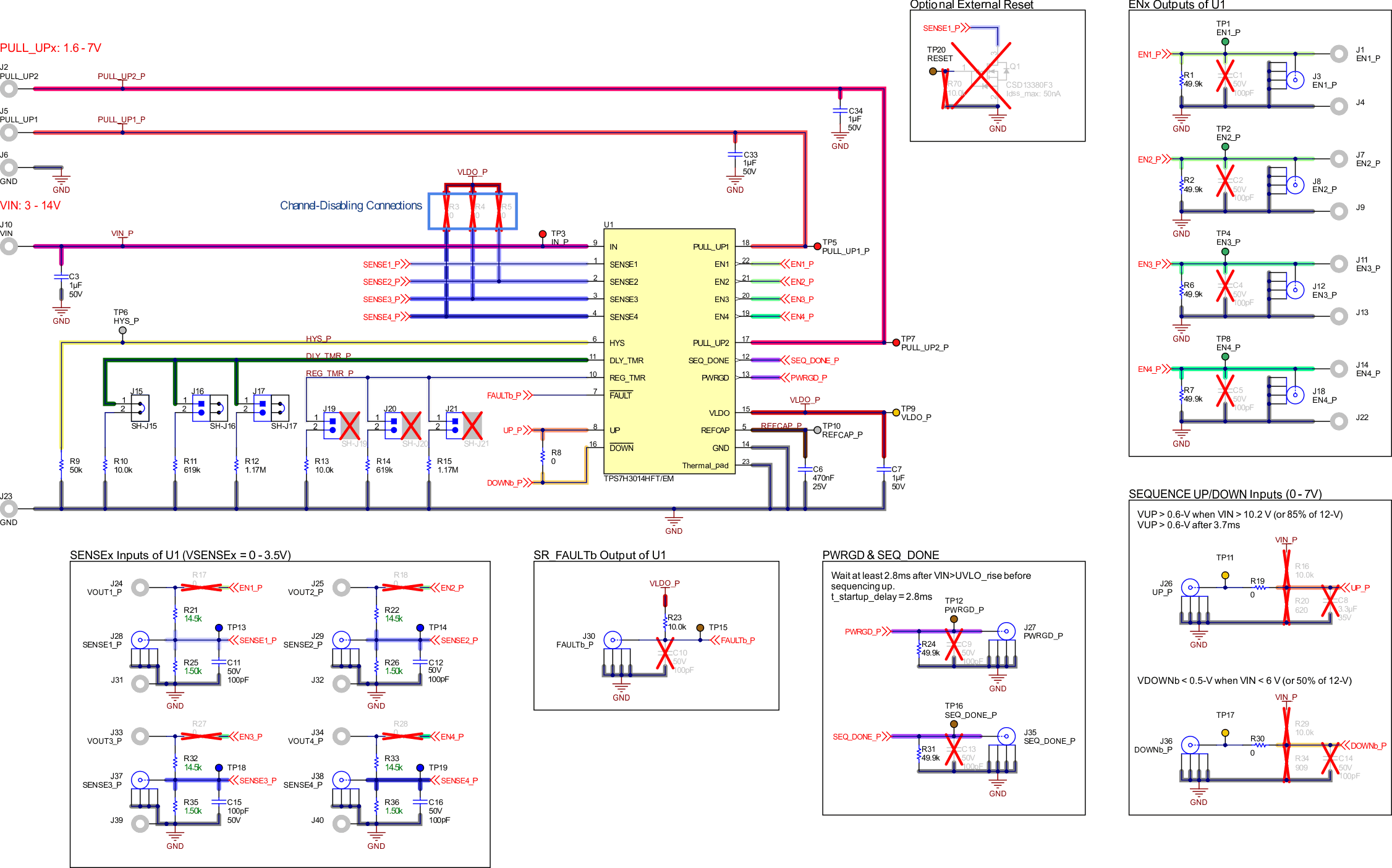
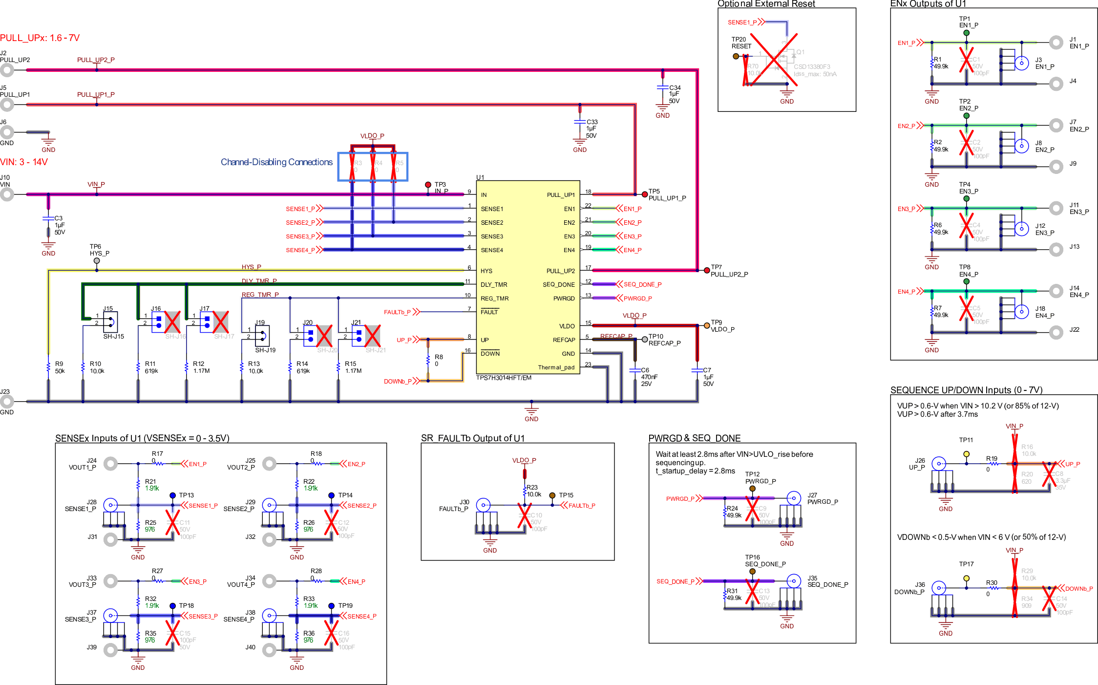
The TPS7H3014-SP is packaged in a 22-pin CFP-HFT ceramic package as shown in Figure 3-1. The TPS7H3014-SP evaluation module was used to evaluate the performance and characteristics of the TPS7H3014-SP under heavy ion radiation. The TPS7H3014EVM-CVAL (Evaluation Module) is shown in Figure 3-2. The actual EVM BOM was modified from the original (or default). The board was configured to be dual-site rather than in daisy-chain. This means both samples on a given board were configured under the same conditions (or configuration). Three different configurations were used during the heavy-ions test campaign, the details are provided on Figure 3-3, Figure 3-4, and Figure 3-5.
![TPS7H3014-SP Photograph of Delidded TPS7H3014-SP [Left] and Pinout Diagram [Right] TPS7H3014-SP Photograph of Delidded TPS7H3014-SP [Left] and Pinout Diagram [Right]](/ods/images/SLVK172/GUID-20240513-SS0I-WSZA-X6IC-IPM7D9WWP89I-low.svg) Figure 3-1 Photograph of Delidded TPS7H3014-SP [Left] and Pinout Diagram [Right]
Figure 3-1 Photograph of Delidded TPS7H3014-SP [Left] and Pinout Diagram [Right] Figure 3-2 TPS7H3014-SP EVM Top View
 Figure 3-3 TPS7H3014-SP EVM Schematic for DSEE Testing
 Figure 3-4 TPS7H3014-SP EVM Schematic for SET Testing
 Figure 3-5 TPS7H3014-SP EVM for Worst-Case SET Testing