SLVS332J March 2001 – December 2016 TPS797
PRODUCTION DATA.
1 Features
- 50-mA Low-Dropout Regulator
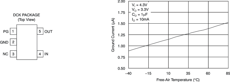
- Ultra-Low 1.2-µA Quiescent Current at 10 mA
- 5-Pin SC70 (DCK) Package
- Integrated Power Good Output
- Stable With Any Capacitor Greater Than 0.47 µF
- Typical Dropout Voltage of 105 mV at 10 mA (TPS79733)
- Over-Current Limitation
- Operating Junction Temperature Range of –40°C to 85°C
2 Applications
- Battery-Powered Microcontrollers and Microprocessors
3 Description
The TPS797xx family of low-dropout voltage regulators (LDOs) offers the benefits of low-dropout voltage and ultra-low-power operation. The device is stable with any capacitor greater than 0.47-µF. Therefore, implementations of this device require very little board space due to the miniaturized packaging and potentially small output capacitor. In addition, the family includes an integrated open drain active-high power good (PG) output. Intended for use in microcontroller-based, battery-powered applications, the TPS797xx family low dropout and ultra-low-power operation result in a significant increase in system battery operating life. The small packaging minimizes consumption of board space.
The device is enabled when the applied voltage exceeds the minimum input voltage. The usual PNP pass transistor has been replaced by a PMOS pass element. Because the PMOS pass element behaves as a low-value resistor, the dropout voltage is very low (typically, 105 mV at 10-mA of load current), and is directly proportional to the load current. The quiescent current is ultra-low (1.2-µA, typically) and is stable over the entire range of output load current
(0 mA to 50 mA). When properly configured with a pullup resistor, the PG output can implement a power-on reset or low-battery indicator.
Device Information(1)
| PART NUMBER | PACKAGE | BODY SIZE (NOM) |
|---|---|---|
| TPS797xx | SC70 (5) | 2.00 mm × 1.25 mm |
- For all available packages, see the orderable addendum at the end of the data sheet.
Ground Current vs Free-Air Temperature
