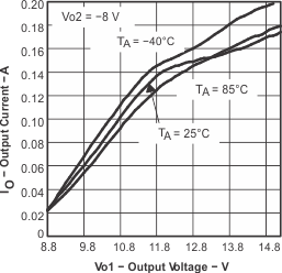
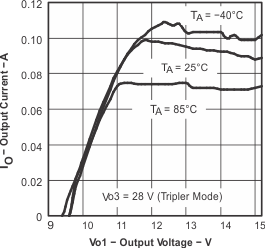
-
TPS6510x Triple Output LCD Supply With Linear Regulator and VCOM Buffer
- 1 Features
- 2 Applications
- 3 Description
- 4 Revision History
- 5 Device Options
- 6 Pin Configuration and Functions
- 7 Specifications
- 8 Detailed Description
- 9 Application and Implementation
- 10Power Supply Recommendations
- 11Layout
- 12Device and Documentation Support
- 13Mechanical, Packaging, and Orderable Information
- IMPORTANT NOTICE
TPS6510x Triple Output LCD Supply With Linear Regulator and VCOM Buffer
1 Features
- 2.7-V to 5.8-V Input Voltage Range
- 1.6-MHz Fixed Switching Frequency
- 3 Independent Adjustable Outputs
- Boost Converter Output Voltage VO1 of up to 15 V With < 1% Output Voltage Accuracy
- Negative Regulated Charge Pump VO2
- Positive Charge Pump VO3
- Integrated VCOM Buffer
- Virtual Synchronous Converter Technology in Boost Converter
- Auxiliary 3.3-V Linear Regulator Controller
- Internal Soft Start
- Internal Power-On Sequencing
- Fault Detection of all Outputs (TPS65100/05)
- No Fault Detection (TPS65101)
- Thermal Shutdown
- Available in TSSOP-24 and VQFN-24 PowerPAD™ Packages
2 Applications
- TFT LCD Displays for Notebooks
- TFT LCD Displays for Monitors
- Portable DVD Players
- Tablet PCs
- Car Navigation Systems
- Industrial Displays
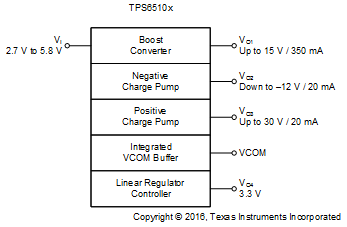
Block Diagram
3 Description
The TPS6510x series offers a compact and small power supply solution that provides all three voltages required by thin film transistor (TFT) LCD displays. The auxiliary linear regulator controller can be used to generate a 3.3-V logic power rail for systems powered by a 5-V supply rail only.
The main output VO1, is a 1.6-MHz, fixed-frequency PWM boost converter providing the source drive voltage for the LCD display. The device is available in two versions with different internal switch current limits to allow the use of a smaller external inductor when lower output power is required. The TPS65100/01 has a typical switch current limit of 2.3 A, and the TPS65105 has a typical switch current limit of 1.37 A. A fully integrated adjustable charge pump doubler/tripler provides the positive LCD gate drive voltage. An externally adjustable negative charge pump provides the negative gate drive voltage. Due to the high 1.6-MHz switching frequency of the charge pumps, inexpensive and small 220-nF capacitors can be used.
The TPS6510x series has an integrated VCOM buffer to power the LCD backplane. For LCD panels powered by 5 V only, the TPS6510x series has a linear regulator controller using an external transistor to provide a regulated 3.3-V output for the digital circuits. For maximum safety, the TPS65100/05 goes into shutdown as soon as one of the outputs is out of regulation. The device can be enabled again by toggling the input or the enable (EN) pin to GND. The TPS65101 does not enter shutdown when one of the outputs is below its power good threshold.
Device Information(1)
| PART NUMBER | PACKAGE | BODY SIZE (NOM) |
|---|---|---|
| TPS6510x | HTSSOP (24) | 7.80 mm × 4.40 mm |
| VQFN (24) | 4.00 mm × 4.00 mm |
- For all available packages, see the orderable addendum at the end of the data sheet.
4 Revision History
Changes from C Revision (April 2006) to D Revision
- Added ESD Ratings table, Thermal Information table, Feature Description section, Device Functional Modes, Application and Implementation section, Power Supply Recommendations section, Layout section, Device and Documentation Support section, and Mechanical, Packaging, and Orderable Information section Go
- Deleted Ordering Information table, see POA at the end of the datasheet. Go
5 Device Options
| LINEAR REGULATOR OUTPUT VOLTAGE | MINIMUM SWITCH CURRENT LIMIT | PACKAGE MARKING |
|---|---|---|
| 3.3 V | 1.6 A | TPS65100 |
| 3.3 V | 1.6 A | TPS65101 |
| 3.3 V | 0.96 A | TPS65105 |
6 Pin Configuration and Functions
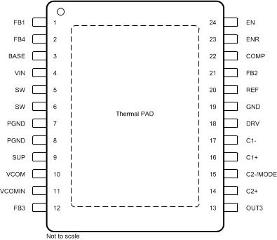

Pin Functions
| PIN | I/O | DESCRIPTION | ||
|---|---|---|---|---|
| NAME | HTSSOP | VQFN | ||
| BASE | 3 | 6 | O | Base drive output for the external transistor. If Linear Regulator is not needed pull this pin against VIN. |
| C1+ | 16 | 19 | — | Positive terminal of the charge pump flying capacitor |
| C1- | 17 | 20 | — | Negative terminal of the charge pump flying capacitor |
| C2+ | 14 | 17 | — | Positive terminal for the charge pump flying capacitor. If the device runs in voltage doubler mode, this pin should be left open. |
| C2-/MODE | 15 | 18 | — | Negative terminal of the charge pump flying capacitor and charge pump MODE pin. If the flying capacitor is connected to this pin, the converter operates in a voltage tripler mode. If the charge pump needs to operate in a voltage doubler mode, the flying capacitor is removed and the C2-/MODE pin should be connected to GND. |
| COMP | 22 | 1 | — | Compensation pin for the main boost converter. A small capacitor is connected to this pin. |
| DRV | 18 | 21 | O | External charge pump driver |
| EN | 24 | 3 | I | Enable pin of the device. This pin should be terminated and not be left floating. A logic high enables the device and a logic low shuts down the device. |
| ENR | 23 | 2 | I | Enable pin of the linear regulator controller. This pin should be terminated and not be left floating. Logic high enables the regulator and a logic low puts the regulator in shutdown. |
| FB1 | 1 | 4 | I | Feedback pin of the boost converter |
| FB2 | 21 | 24 | I | Feedback pin of negative charge pump |
| FB3 | 12 | 15 | I | Feedback pin of positive charge pump |
| FB4 | 2 | 5 | I | Feedback pin of the linear regulator controller. The linear regulator controller is set to a fixed output voltage of 3.3 V or 3 V depending on the version. |
| GND | 19 | 22 | — | Ground |
| OUT3 | 13 | 16 | O | Positive charge pump output |
| PGND | 7, 8 | 10, 11 | — | Power ground |
| REF | 20 | 23 | O | Internal reference output typically 1.23 V |
| SUP | 9 | 12 | I | Supply pin of the positive, negative charge pump, boost converter gate drive circuit, and VCOM buffer. This pin should be connected to the output of the main boost converter and cannot be connected to any other voltage source. For performance reasons, it is not recommended for a bypass capacitor to be connected directly to this pin. |
| SW | 5, 6 | 8, 9 | — | Switch pin of the boost converter |
| VCOM | 10 | 13 | O | VCOM buffer output |
| VCOMIN | 11 | 14 | I | Positive input terminal of the VCOM buffer. When the VCOM buffer is not used, this terminal can be connected to GND to reduce the overall quiescent current of the IC. |
| VIN | 4 | 7 | I | Input voltage pin of the device |
| PowerPAD™/ Thermal Die |
— | — | — | The PowerPAD or exposed thermal die needs to be connected to the power ground pins (PGND) |
7 Specifications
7.1 Absolute Maximum Ratings
Over operating free-air temperature range (unless otherwise noted)(1)| MIN | MAX | UNIT | |
|---|---|---|---|
| Voltages on pin VIN(2) | –0.3 | 6 | V |
| Voltages on pin SUP, PG (2) | –0.3 | 15.5 | V |
| Voltage on pin FB1, FB2, FB3, FB4 | –0.3 | 5.5 | V |
| Voltages on pin EN, MODE, ENR(2) | –0.3 | VI + 0.3 | V |
| Voltage on VCOMIN | –0.3 | 14 | V |
| Voltage on pin SW(2) | –0.3 | 20 | V |
| Voltage on pin DRV | –0.3 | 15 | V |
| Voltage on pin REF | –0.3 | 4 | V |
| Voltage on pin BASE | –0.3 | 5.5 | V |
| Voltage on pin VOUT3 | –0.3 | 30 | V |
| Voltage on pin VCOM | –0.3 | 15 | V |
| Voltage on pin C1+, C2+ | –0.3 | 30 | V |
| Voltage on pin C1–, C2– | –0.3 | 15 | V |
| Continuous power dissipation | See Dissipation Ratings | ||
| Operating junction temperature, TJ | –40 | 150 | °C |
| Storage temperature, Tstg | –65 | 150 | °C |
7.2 ESD Ratings
| VALUE | UNIT | |||
|---|---|---|---|---|
| V(ESD) | Electrostatic discharge | Human-body model (HBM), per ANSI/ESDA/JEDEC JS-001(1) | ±2000 | V |
| Charged-device model (CDM), per JEDEC specification JESD22-C101(2) | ±500 | |||
7.3 Recommended Operating Conditions
| MIN | NOM | MAX | UNIT | ||
|---|---|---|---|---|---|
| VI | Input voltage | 2.7 | 5.8 | V | |
| L | Inductor(1) | 4.7 | µH | ||
| TA | Operating free-air temperature | –40 | 85 | °C | |
| TJ | Operating junction temperature | –40 | 125 | °C | |
7.4 Thermal Information
| THERMAL METRIC(1) | TPS6510x | UNIT | ||
|---|---|---|---|---|
| PWP (HTSSOP) | RGE (VQFN) | |||
| 24 PINS | 24 PINS | |||
| RθJA | Junction-to-ambient thermal resistance | 37.2 | 33 | °C/W |
| RθJC(top) | Junction-to-case (top) thermal resistance | 18.9 | 35.3 | °C/W |
| RθJB | Junction-to-board thermal resistance | 16.4 | 10.7 | °C/W |
| ψJT | Junction-to-top characterization parameter | 0.4 | 0.4 | °C/W |
| ψJB | Junction-to-board characterization parameter | 16.2 | 10.8 | °C/W |
| RθJC(bot) | Junction-to-case (bottom) thermal resistance | 2.1 | 1.8 | °C/W |
7.5 Electrical Characteristics
VI = 3.3 V, EN = VI, VO1 = 10 V, TA = –40°C to 85°C, typical values are at TA = 25°C (unless otherwise noted)| PARAMETER | TEST CONDITIONS | MIN | TYP | MAX | UNIT | |
|---|---|---|---|---|---|---|
| SUPPLY CURRENT | ||||||
| VI | Input voltage range | 2.7 | 5.8 | V | ||
| II(VIN) | Quiescent current (VIN) | ENR = VCOMIN = GND, VO3 = 2 × VO1
Boost converter not switching |
0.7 | 0.9 | mA | |
| II(QCharge) | Charge pump quiescent current (SUP) | VO1 = SUP = 10 V, VO3 = 2 × VO1 | 1.7 | 2.7 | mA | |
| VO1 = SUP = 10 V, VO3 = 3 × VO1 | 3.9 | 6 | ||||
| II(QVCOM) | VCOM quiescent current (SUP) | ENR = GND, VO1 = SUP = 10 V | 750 | 1300 | µA | |
| II(QEN) | LDO controller quiescent current (VIN) | ENR = VI, EN = GND | 300 | 800 | µA | |
| II(sd) | Shutdown current (VIN) | EN = ENR = GND | 1 | 10 | µA | |
| VIT– | Undervoltage lockout threshold | VI falling | 2.2 | 2.4 | V | |
| Thermal shutdown temperature threshold | TJ rising | 160 | °C | |||
| LOGIC SIGNALS | ||||||
| VIH | High-level input voltage (EN, ENR) | 1.5 | V | |||
| VIL | Low-level input voltage (EN, ENR) | 0.4 | V | |||
| IIH , IIL | Input leakage current | EN = ENR = GND or VI | 0.01 | 0.1 | µA | |
| MAIN BOOST CONVERTER VO1 | ||||||
| VO1 | Output voltage range | 5 | 15 | V | ||
| VO1 – VI | Minimum input to output voltage difference |
1 | V | |||
| V(REF) | Reference output voltage (REF) | 1.205 | 1.213 | 1.219 | V | |
| Vref | Feedback regulation voltage (FB1) | 1.136 | 1.146 | 1.154 | V | |
| IIB | Feedback input bias current | 10 | 100 | nA | ||
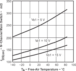
| rDS(on) | N-MOSFET on-resistance (Q1) | VO1 = 10 V, I(sw) = 500 mA | 195 | 290 | mΩ | |
| VO1 = 5 V, I(sw) = 500 mA | 285 | 420 | ||||
| ILIM | N-MOSFET switch current limit (Q1) | TPS65100, TPS65101 | 1.6 | 2.3 | 2.6 | A |
| TPS65105 | 0.96 | 1.37 | 1.56 | A | ||
| rDS(on) | P-MOSFET on-resistance (Q2) | VO1 = 10 V, I(sw) = 100 mA | 9 | 15 | Ω | |
| VO1 = 5 V, I(sw) = 100 mA | 14 | 22 | ||||
| Maximum P-MOSFET peak switch current | 1 | A | ||||
| I(SW)(off) | Off-state current (SW) | V(sw) = 15 V | 1 | 10 | µA | |
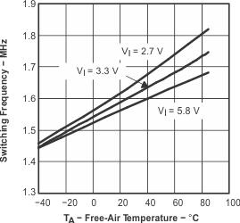
| fOSC | Oscillator frequency | 0°C ≤ TA ≤ 85°C | 1.295 | 1.6 | 2.1 | MHz |
| –40°C ≤ TA ≤ 85°C | 1.191 | 1.6 | 2.1 | |||
| ΔVO(ΔVI) | Line regulation | 2.7 V ≤ VI ≤ 5.7 V, Iload = 100 mA | 0.012 | %/V | ||
| ΔVO(ΔIO) | Load regulation | 0 mA ≤ IO ≤ 300 mA | 0.2 | %/A | ||
| NEGATIVE CHARGE PUMP VO2 | ||||||
| VO2 | Output voltage range | –2 | V | |||
| V(REF) | Reference output voltage (REF) | 1.205 | 1.213 | 1.219 | V | |
| Vref | Feedback regulation voltage (FB2) | –36 | 0 | 36 | mV | |
| IIB | Feedback input bias current | 10 | 100 | nA | ||
| rDS(on) | Q8 P-Channel switch rDS(ON) | IO = 20 mA | 4.3 | 8 | Ω | |
| Q9 N-Channel switch rDS(ON) | 2.9 | 4.4 | ||||
| IOM | Maximum output current | 20 | mA | |||
| ΔVO(ΔVI) | Line regulation | 7 V ≤ VO1 ≤ 15 V, IO = 10 mA, VO2 = –5 V | 0.09 | %/V | ||
| ΔVO(ΔIO) | Load regulation | 1 mA ≤ IO ≤ 20 mA, VO2 = –5 V | 0.126 | %/mA | ||
| POSITIVE CHARGE PUMP VO3 | ||||||
| VO3 | Output voltage range | 30 | V | |||
| V(REF) | Reference output voltage | 1.205 | 1.213 | 1.219 | V | |
| Vref | Feedback regulation voltage (FB3) | 1.187 | 1.214 | 1.238 | V | |
| IIB | Feedback input bias current | 10 | 100 | nA | ||
| rDS(on) | Q3 P-Channel switch rDS(on) | IO = 20 mA | 9.9 | 15.5 | Ω | |
| Q4 N-Channel switch rDS(on) | 1.1 | 1.8 | ||||
| Q5 P-Channel switch rDS(on) | 4.6 | 8.5 | ||||
| Q6 N-Channel switch rDS(on) | 1.2 | 2.2 | ||||
| Vd | D1 – D4 Shottky diode forward voltage | I(D1-D4) = 40 mA | 610 | 720 | mV | |
| IOM | Maximum output current | 20 | mA | |||
| ΔVO(ΔVI) | Line regulation | 10 V ≤ VO1 ≤ 15 V, IO = 10 mA, VO3 = 27 V | 0.56 | %/V | ||
| ΔVO(ΔIO) | Load regulation | 1 mA ≤ IO ≤ 20 mA, VO3 = 27 V | 0.05 | %/mA | ||
| LINEAR REGULATOR CONTROLLER VO4 | ||||||
| VO4 | Output voltage range (FB4) | 4.5 V ≤ VI ≤ 5.5 V, 10 mA ≤ IO ≤ 500 mA | 3.2 | 3.3 | 3.4 | V |
| I(BASE) | Maximum base drive current | VI – VO4 – VBE ≥ 0.5 V (1) | 13.5 | 19 | mA | |
| VI – VO4 – VBE ≥ 0.75 V (1) | 20 | 27 | ||||
| ΔVO(ΔVI) | Line regulation | 4.75 V ≤ VI ≤ 5.5 V, IO = 500 mA | 0.186 | %/V | ||
| ΔVO(ΔIO) | Load regulation | 1 mA ≤ IO ≤ 500 mA, VI = 5 V | 0.064 | %/A | ||
| Start-up current | VO4 ≤ 0.8 V | 11 | 20 | 25 | mA | |
| VCOM BUFFER | ||||||
| Vcm | Common mode input range | 2.25 | VO1-2 | V | ||
| VIo | Input offset voltage (IN) | IO = 0 mA | –25 | 25 | mV | |
| ΔVO(ΔIO) | DC Load regulation | IO = ±25 mA | –30 | 37 | mV | |
| IO = ±50 mA | –45 | 55 | ||||
| IO = ±100 mA | –72 | 85 | ||||
| IO = ±150 mA | –97 | 110 | ||||
| IIB | Input bias current (IN) | –300 | –30 | 300 | nA | |
| IOM | Peak output current | VO1 = 15 V | 1.2 | A | ||
| VO1 = 10 V | 0.65 | A | ||||
| VO1 = 5 V | 0.15 | A | ||||
| FAULT PROTECTION THRESHOLDS | ||||||
| V(th, VO1) | Shutdown threshold | VO1 Rising | –12% VO1 | –8.75% VO1 | –6 VO1 | V |
| V(th, VO2) | VO2 Rising | –13 VO2 | –9% VO2 | –5 VO2 | V | |
| V(th, VO3) | VO3 Rising | –11 VO3 | –8% VO3 | –5 VO3 | V | |
7.6 Dissipation Ratings
| PACKAGE | RΘJA | TA ≤ 25°C POWER RATING |
TA = 70°C POWER RATING |
TA = 85°C POWER RATING |
|---|---|---|---|---|
| 24-Pin TSSOP | 30.13 C°/W (PWP soldered) | 3.3 W | 1.83 W | 1.32 W |
| 24-Pin VQFN | 30 C°/W | 3.3 W | 1.8 W | 1.3 W |
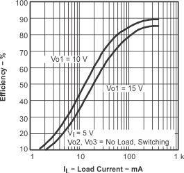
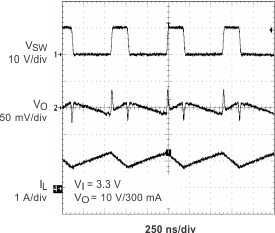
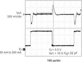
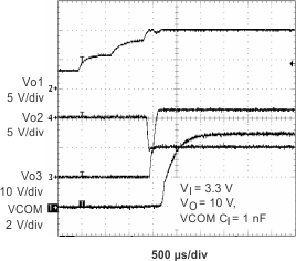
7.7 Typical Characteristics
