SLVS530D SEPTEMBER   2005  – October 2015 TPS63700

PRODUCTION DATA.  

  1. Features
  2. Applications
  3. Description
  4. Revision History
  5. Pin Configuration and Functions
  6. Specifications
    1. 6.1 Absolute Maximum Ratings
    2. 6.2 ESD Ratings
    3. 6.3 Recommended Operating Conditions
    4. 6.4 Thermal Information
    5. 6.5 Electrical Characteristics
    6. 6.6 Typical Characteristics
  7. Detailed Description
    1. 7.1 Overview
    2. 7.2 Functional Block Diagram
    3. 7.3 Feature Description
      1. 7.3.1 Enable
      2. 7.3.2 Load Disconnect
      3. 7.3.3 Output Overvoltage Protection
      4. 7.3.4 Undervoltage Lockout
      5. 7.3.5 Overtemperature Shutdown
    4. 7.4 Device Functional Modes
      1. 7.4.1 Soft-Start
      2. 7.4.2 PWM Operation
      3. 7.4.3 Power Save Mode Operation
      4. 7.4.4 Control
  8. Application and Implementation
    1. 8.1 Application Information
    2. 8.2 Typical Application
      1. 8.2.1 Design Requirements
      2. 8.2.2 Detailed Design Procedure
        1. 8.2.2.1 Programming the Output Voltage: Converter
          1. 8.2.2.1.1 Inductor Selection
        2. 8.2.2.2 Capacitor Selection
          1. 8.2.2.2.1 Input Capacitor
          2. 8.2.2.2.2 Output Capacitors
        3. 8.2.2.3 Stabilizing the Control Loop
          1. 8.2.2.3.1 Feedback Divider
          2. 8.2.2.3.2 Compensation Capacitor
      3. 8.2.3 Application Curves
    3. 8.3 System Example
  9. Power Supply Recommendations
  10. 10Layout
    1. 10.1 Layout Guidelines
    2. 10.2 Layout Example
  11. 11Device and Documentation Support
    1. 11.1 Device Support
      1. 11.1.1 Third-Party Products Disclaimer
    2. 11.2 Community Resources
    3. 11.3 Trademarks
    4. 11.4 Electrostatic Discharge Caution
    5. 11.5 Glossary
  12. 12Mechanical, Packaging, and Orderable Information

5 Pin Configuration and Functions

DRC Package
10-Pin VSON With PowerPAD™
Top View
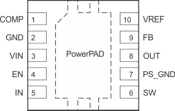
TPS63700 po_lvs530.gif

Pin Functions

PIN I/O DESCRIPTION
NAME NO.
COMP 1 I/O Compensation pin for control, connect a 4.7 nF capacitor between this pin and GND
GND 2 Ground pin
VIN 3 I Supply voltage input for control logic, connect a RC circuit of 10R and 100 nF to filter this supply voltage
EN 4 I Enable pin (EN = GND: disabled; EN = VIN: enabled)
IN 5 I Supply voltage for the power switch
SW 6 O Inverter switch output
PS_GND 7 I Connect to GND for control logic
OUT 8 I Output voltage sense input
FB 9 I Feedback pin for the voltage divider
VREF 10 O Reference voltage output. Connect a 220-nF capacitor to ground. Connect the lower resistor of the negative output voltage divider to this pin.