SLVS555N November 2004 – June 2024 TLVH431 , TLVH431A , TLVH431B , TLVH432 , TLVH432A , TLVH432B
PRODUCTION DATA
- 1
- 1 Features
- 2 Applications
- 3 Description
- 4 Pin Configuration and Functions
- 5 Specifications
- 6 Parameter Measurement Information
- 7 Detailed Description
- 8 Applications and Implementation
- 9 Device and Documentation Support
- 10Revision History
- 11Mechanical, Packaging, and Orderable Information
3 Description
The TLVH431 and TLVH432 devices are low-voltage 3-terminal adjustable voltage references, with specified thermal stability over applicable industrial and commercial temperature ranges. Output voltage can be set to any value between VREF (1.24V) and 18V with two external resistors (see Figure 6-2). These devices operate from a lower voltage (1.24V) than the widely used TL431 and TL1431 shunt-regulator references.
When used with an optocoupler, the TLVH431 and TLVH432 devices are an excellent choice for voltage references in isolated feedback circuits for 3V to 3.3V switching-mode power supplies. The devices have a typical output impedance of 0.25Ω. Active output circuitry provides a very sharp turn-on characteristic, making the TLVH431 and TLVH432 devices excellent replacements for low-voltage Zener diodes in many applications, including on-board regulation and adjustable power supplies.
The TLVH432 device is identical to the TLVH431 device, but is offered with different pinouts for the
3-pin SOT-23 and SOT-89 packages.
| PART NUMBER | PACKAGE (1) | BODY SIZE (NOM) (2) |
|---|---|---|
| TLVH43xxDBV | SOT-23 (5) | 2.90mm × 1.60mm |
| TLVH43xxDBZ | SOT-23 (3) | 2.92mm × 1.30mm |
| TLVH43xxDCK | SC70 (6) | 2.00mm × 1.25mm |
| TLVH43xxLP | TO-92 (3) | 4.30mm × 4.30mm |
| TLVH43xxPK | SOT-89 (3) | 4.50mm × 2.50mm |
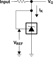
 Simplified Schematic