SLVS610C August 2006 – October 2024 TL2842B , TL2843B , TL2844B , TL2845B , TL3842B , TL3843B , TL3844B , TL3845B
PRODUCTION DATA
- 1
- 1 Features
- 2 Applications
- 3 Description
- 4 Pin Configuration and Functions
-
5 Specifications
- 5.1 Absolute Maximum Ratings
- 5.2 ESD Ratings
- 5.3 Recommended Operating Conditions
- 5.4 Thermal Information
- 5.5 Reference Section Electrical Characteristics
- 5.6 Oscillator Section Electrical Characteristics
- 5.7 Error-Amplifier Section Electrical Characteristics
- 5.8 Current-Sense Section Electrical Characteristics
- 5.9 Output Section Electrical Characteristics
- 5.10 Undervoltage-Lockout Section Electrical Characteristics
- 5.11 Pulse-Width Modulator Section Electrical Characteristics
- 5.12 Supply Voltage Electrical Characteristics
- 5.13 Typical Characteristics
- 6 Detailed Description
- 7 Application and Implementation
- 8 Device and Documentation Support
- 9 Revision History
- 10Mechanical, Packaging, and Orderable Information
3 Description
The TL284xB and TL384xB series of control integrated circuits provide the features that are necessary to implement off-line or dc-to-dc fixed-frequency current-mode control schemes, with a minimum number of external components. Internally implemented circuits include an undervoltage lockout (UVLO) and a precision reference that is trimmed for accuracy at the error amplifier input. Other internal circuits include logic to ensure latched operation, a pulse-width modulation (PWM) comparator that also provides current-limit control, and a totem-pole output stage designed to source or sink high-peak current. The output stage, suitable for driving N-channel MOSFETs, is low when the output stage is in the off state.
The TL284xB and TL384xB series are pin compatible with the standard TL284x and TL384x with the following improvements. The start-up current is specified to be 0.5mA (max), while the oscillator discharge current is trimmed to 8.3mA (typ). In addition, during undervoltage lockout conditions, the output has a maximum saturation voltage of 1.2V while sinking 10mA (VCC = 5V).
Major differences between members of these series are the UVLO thresholds and maximum duty-cycle ranges. Typical UVLO thresholds of 16V (on) and 10V (off) on the TLx842B and TLx844B devices make them ideally suited to off-line applications. The corresponding typical thresholds for the TLx843B and TLx845B devices are 8.4V (on) and 7.6V (off). The TLx842B and TLx843B devices can operate to duty cycles approaching 100%. A duty-cycle range of 0% to 50% is obtained by the TLx844B and TLx845B by the addition of an internal toggle flip-flop, which blanks the output off every other clock cycle. The TL284xB-series devices are characterized for operation from –40°C to 85°C. The TL384xB-series devices are characterized for operation from 0°C to 70°C.
| PART NUMBER | PACKAGE(1) | PACKAGE SIZE(2) |
|---|---|---|
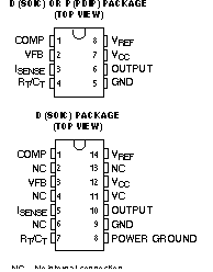
| TLx84x | D (SOIC, 8) | 4.90mm × 6.00mm |
| D (SOIC, 14) | 8.65mm × 6.00mm | |
| P (PDIP, 8) | 9.81mm × 9.43mm |
