SLVS675E August   2006  – January 2024 TPS5410

PRODUCTION DATA  

  1.   1
  2. Features
  3. Applications
  4. Description
  5. Pin Configuration and Functions
  6. Specifications
    1. 5.1 Absolute Maximum Ratings
    2. 5.2 ESD Ratings
    3. 5.3 Recommended Operating Conditions
    4. 5.4 Thermal Information 
    5. 5.5 Electrical Characteristics
    6. 5.6 Typical Characteristics
  7. Detailed Description
    1. 6.1 Overview
    2. 6.2 Functional Block Diagram
    3. 6.3 Feature Description
      1. 6.3.1  Oscillator Frequency
      2. 6.3.2  Voltage Reference
      3. 6.3.3  Enable (ENA) and Internal Slow-Start
      4. 6.3.4  Undervoltage Lockout (UVLO)
      5. 6.3.5  Boost Capacitor (BOOT)
      6. 6.3.6  Output Feedback (VSENSE)
      7. 6.3.7  Internal Compensation
      8. 6.3.8  Voltage Feed-Forward
      9. 6.3.9  Pulse-Width-Modulation (PWM) Control
      10. 6.3.10 Overcurrent Limiting
      11. 6.3.11 Overvoltage Protection
      12. 6.3.12 Thermal Shutdown
    4. 6.4 Device Functional Modes
      1. 6.4.1 Minimum Input Voltage
      2. 6.4.2 ENA Control
  8. Applications and Implementation
    1. 7.1 Application Information
    2. 7.2 Typical Applications
      1. 7.2.1 Application Circuit
        1. 7.2.1.1 Design Requirements
        2. 7.2.1.2 Detailed Design Procedure
          1. 7.2.1.2.1 Switching Frequency
          2. 7.2.1.2.2 Input Capacitors
          3. 7.2.1.2.3 Output Filter Components
            1. 7.2.1.2.3.1 Inductor Selection
            2. 7.2.1.2.3.2 Capacitor Selection
          4. 7.2.1.2.4 Output Voltage Setpoint
          5. 7.2.1.2.5 Boot Capacitor
          6. 7.2.1.2.6 Catch Diode
          7. 7.2.1.2.7 Advanced Information
            1. 7.2.1.2.7.1 Output Voltage Limitations
            2. 7.2.1.2.7.2 Internal Compensation Network
            3. 7.2.1.2.7.3 Thermal Calculations
        3. 7.2.1.3 Application Curves
      2. 7.2.2 Using All Ceramic Capacitors
        1. 7.2.2.1 Design Requirements
        2. 7.2.2.2 Detailed Design Procedure
          1. 7.2.2.2.1 Output Filter Capacitor Selection
          2. 7.2.2.2.2 External Compensation Network
        3. 7.2.2.3 Application Curves
    3. 7.3 Power Supply Recommendations
    4. 7.4 Layout
      1. 7.4.1 Layout Guidelines
      2. 7.4.2 Layout Example
  9. Device and Documentation Support
    1. 8.1 Documentation Support
      1. 8.1.1 Related Documentation
    2. 8.2 Receiving Notification of Documentation Updates
    3. 8.3 Support Resources
    4. 8.4 Trademarks
    5. 8.5 Electrostatic Discharge Caution
    6. 8.6 Glossary
  10. Revision History
  11. 10Mechanical, Packaging, and Orderable Information

Using All Ceramic Capacitors

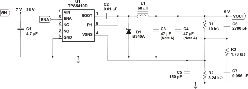
Figure 7-10 shows an application circuit using all ceramic capacitors for the input and output filters. The design procedure is similar to those given for the design example, except for the selection of the output filter capacitor values and the design of the additional compensation components required to stabilize the circuit.
GUID-5FD0BC9F-FC03-40F2-8BA1-D5E0BA4F5CC5-low.gif
C3, C4 = Ceramic TDKC4532X5R1A476MT
Figure 7-10 7-V — 36-V Input to 5-V Output Application Circuit with Ceramic Capacitors