SLVS710C January 2007 – February 2017 TPS65050
PRODUCTION DATA.
- 1 Features
- 2 Applications
- 3 Description
- 4 Revision History
- 5 Device Options
- 6 Pin Configuration and Functions
- 7 Specifications
-
8 Detailed Description
- 8.1 Overview
- 8.2 Functional Block Diagrams
- 8.3
Feature Description
- 8.3.1 Operation of DCDC Converters
- 8.3.2 Power-Save Mode
- 8.3.3 Dynamic Voltage Positioning
- 8.3.4 Soft Start
- 8.3.5 100% Duty Cycle Low Dropout Operation
- 8.3.6 Undervoltage Lockout
- 8.3.7 Mode Selection
- 8.3.8 Enable
- 8.3.9 RESET
- 8.3.10 Push-Button ON-OFF (PB-ON-OFF)
- 8.3.11 Short-Circuit Protection
- 8.3.12 Thermal Shutdown
- 8.3.13 Low Dropout Voltage Regulators
- 8.4 Device Functional Modes
-
9 Application and Implementation
- 9.1 Application Information
- 9.2 Typical Application
- 10Power Supply Recommendations
- 11Layout
- 12Device and Documentation Support
- 13Mechanical, Packaging, and Orderable Information
9 Application and Implementation
NOTE
Information in the following applications sections is not part of the TI component specification, and TI does not warrant its accuracy or completeness. TI’s customers are responsible for determining suitability of components for their purposes. Customers should validate and test their design implementation to confirm system functionality.
9.1 Application Information
This device integrates two step-down converters and four LDOs, which can be used to power the voltage rails needed by a processor or any other application. The PMIC can be controlled through the ENABLE and MODE pins or sequenced from the VIN using RC delay circuits. There is a logic output, RESET, provide the application processor or load a logic signal indicating power good or reset.
9.2 Typical Application
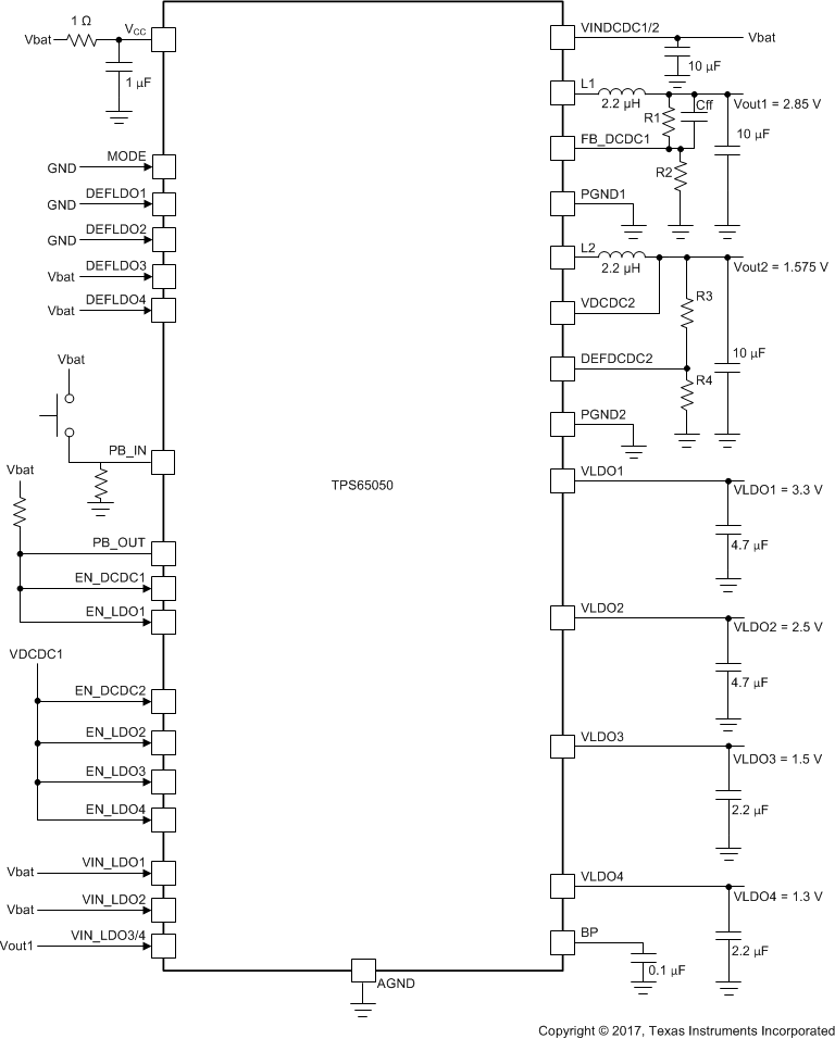 Figure 15. Typical Example Application With PB_ON/OFF Circuit
9.2.1 Design Requirements
Table 2 lists the design requirements for this example.
Table 2. Design Parameters
| PARAMETER | VALUE |
|---|---|
| DCDC1 and DCDC2 input voltage | 2.5 V to 6 V |
| DCDC1 output voltage | 2.85 V |
| DCDC1 output current | 600 mA |
| DCDC2 output voltage | 1.575 V |
| DCDC2 output current | 600 mA |
| LDO1 output voltage | 3.3 V |
| LDO1 output current | 400 mA |
| LDO2 output voltage | 2.5 V |
| LDO2 output current | 400 mA |
| LDO3 output voltage | 1.5 V |
| LDO3 output current | 200 mA |
| LDO4 output voltage | 1.3 V |
| LDO4 output current | 200 mA |
9.2.2 Detailed Design Procedure
9.2.2.1 Output Voltage Setting
9.2.2.1.1 Converter 1 (DCDC1)
The output voltage of converter 1 can be set by an external resistor network. The output voltage can be calculated using Equation 4.

with an internal reference voltage Vref, 0.6 V .
TI recommends setting the total resistance of R1 + R2 to less than 1 MΩ. The resistor network connects to the input of the feedback amplifier, therefore, requiring a small feedforward capacitor in parallel to R1. A typical value of 47 pF is sufficient.
For the TPS65052 and TPS65056 devices, the DCDC1 output voltage is internally fixed to 3.3 V.
9.2.2.1.2 Converter 2 (DCDC2)
The output voltage of converter 2 can be selected as following:
- Adjustable output voltage defined with external resistor network on pin DEFDCDC2. This option is available for the TPS65050 and TPS65051 devices.
- Two default fixed output voltages are selectable by pin DEFDCDC2 (see Table 3). This option is available for the TPS65052, TPS65054, and TPS65056 devices.
Table 3. Default Fixed Output Voltages
| Converter 2 | DEFDCDC2 = low | DEFDCDC2 = high |
|---|---|---|
| TPS65050 | — | — |
| TPS65051 | — | — |
| TPS65052 | 1 V | 1.3 V |
| TPS65054 | 1.3 V | 1.05 V |
| TPS65056 | 1 V | 1.3 V |
The adjustable output voltage can be calculated similarly to the DCDC1 converter. Setting the total resistance of R3 + R4 to less than 1 MΩ is recommended. Route the DEFDCDC2 line separate from noise sources, such as the inductor or the L2 line. The VDCDC2 line needs to be directly connected to the output capacitor. As the VDCDC2 line is the feedback to the internal amplifier, no feedforward capacitor at R3 is needed.
Using an external resistor divider at DEFDCDC2:
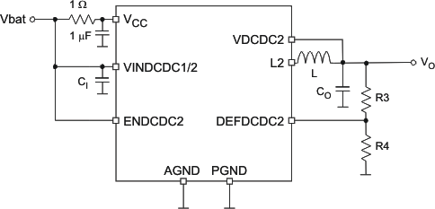 Figure 16. External Resistor Divider
V(DEFDCDC2) = 0.6 V

See Table 4 for typical resistor values:
Table 4. Typical Resistor Values
| OUTPUT VOLTAGE | R1 | R2 | NOMINAL VOLTAGE | Typical CFF |
|---|---|---|---|---|
| 3.3 V | 680 kΩ | 150 kΩ | 3.32 V | 47 pF |
| 3 V | 510 kΩ | 130 kΩ | 2.95 V | 47 pF |
| 2.85 V | 560 kΩ | 150 kΩ | 2.84 V | 47 pF |
| 2.5 V | 510 kΩ | 160 kΩ | 2.51 V | 47 pF |
| 1.8 V | 300 kΩ | 150 kΩ | 1.8 v | 47 pF |
| 1.6 V | 200 kΩ | 120 kΩ | 1.6 V | 47 pF |
| 1.5 V | 300 kΩ | 200 kΩ | 1.5 V | 47 pF |
| 1.2 V | 330 kΩ | 330 kΩ | 1.2 V | 47 pF |
9.2.2.2 Output Filter Design (Inductor and Output Capacitor)
9.2.2.2.1 Inductor Selection
The two converters operate with 2.2-μH output inductor. Larger or smaller inductor values can be used to optimize the performance of the device for specific operation conditions. The selected inductor has to be rated for its DC resistance and saturation current. The DC resistance of the inductance directly influences the efficiency of the converter. Therefore, an inductor with lowest DC resistance should be selected for highest efficiency. The minimum inductor value is 1.5 μH, but an output capacitor of 22 μF minimum is needed in this case. For an output voltage above 2.8 V, TI recommends an inductor value of 3.3 μH (minimum). Lower values result in an increased output voltage ripple in PFM mode.
Use Equation 6 to calculate the maximum inductor current under static load conditions. The saturation current of the inductor should be rated greater than the maximum inductor current as calculated with Equation 6. TI recommends this because during heavy load transient the inductor current rises above the calculated value.

where
- f = Switching Frequency (2.25-MHz typical)
- L = Inductor Value
- Δ IL= Peak-to-peak inductor ripple current
- ILmax = Maximum Inductor current
The highest inductor current occurs at maximum VI. Open core inductors have a soft saturation characteristic, and they can normally handle greater inductor currents versus a comparable shielded inductor.
A more conservative approach is to select the inductor current rating just for the maximum switch current of the corresponding converter. Consideration must be given to the difference in the core material from inductor to inductor which has an impact on the efficiency especially at high switching frequencies. See Table 5 and the typical applications for possible inductors.
Table 5. Tested Inductors
| INDUCTOR TYPE | INDUCTOR VALUE | SUPPLIER |
|---|---|---|
| LPS3010 | 2.2 μH | Coilcraft |
| LPS3015 | 3.3 μH | Coilcraft |
| LPS4012 | 2.2 μH | Coilcraft |
| VLF4012 | 2.2 μH | TDK |
9.2.2.2.2 Output Capacitor Selection
The advanced Fast Response voltage mode control scheme of the two converters allows the use of small ceramic capacitors with a value of 22-μF (typical) without having large output voltage undershoots and overshoots during heavy load transients. Ceramic capacitors having low ESR values result in lowest output voltage ripple, and are recommended.
If ceramic output capacitors are used, the capacitor RMS ripple current rating always meets the application requirements. For completeness, the RMS ripple current is calculated as:

At nominal load current, the inductive converters operate in PWM mode, and the overall output voltage ripple is the sum of the voltage spike caused by the output capacitor ESR plus the voltage ripple caused by charging and discharging the output capacitor:

where
- the highest output voltage ripple occurs at the highest input voltage VI
At light load currents, the converters operate in Power-Save Mode and the output voltage ripple is dependent on the output capacitor value. The output voltage ripple is set by the internal comparator delay and the external capacitor. The typical output voltage ripple is less than 1% of the nominal output voltage.
9.2.2.2.3 Input Capacitor Selection
Because of the nature of the buck converter having a pulsating input current, a low ESR input capacitor is required for best input voltage filtering and minimizing the interference with other circuits caused by high input voltage spikes. The converters need a ceramic input capacitor of 10 μF. The input capacitor can be increased without any limit for better input voltage filtering.
Table 6. Possible Capacitors
| CAPACITOR VALUE | SIZE | SUPPLIER | TYPE |
|---|---|---|---|
| 2.2 μF | 0805 | TDK C2012X5R0J226MT | Ceramic |
| 2.2 μF | 0805 | Taiyo Yuden JMK212BJ226MG | Ceramic |
| 10 μF | 0805 | Taiyo Yuden JMK212BJ106M | Ceramic |
| 10 μF | 0805 | TDK C2012X5R0J106M | Ceramic |
| 10 μF | 0603 | Taiyo Yuden JMK107BJ106MA | Ceramic |
9.2.2.3 Low Drop Out Voltage Regulators (LDOs)
The output voltage of all 4 LDOs in the TPS65051, TPS65054, and TPS65056 devices are set by an external resistor network. The output voltage is calculated using Equation 9.

where
- an internal reference voltage, Vref, 1 V (typical)
TI recommends setting the total resistance of R5 + R6 to less than 1 MΩ. Typically, there is no feedforward capacitor needed at the voltage dividers for the LDOs.

Typical resistor values:
Table 7. Typical Resistor Values
9.2.2.4 PB-ONOFF and Sequencing
The PB-ONOFF output can be used to enable one or several converters. After power up, the PB_OUT pin is low, and pulls down the enable pins connected to PB_OUT; EN_DCDC1, and EN_LDO1 in Figure 15. When PB_IN is pulled to VCC for longer than 32 ms, the PB_OUT pin is turned off, hence the enable pins pulled high using a pullup resistor to VCC. This enables the DCDC1 converter and LDO1. The output voltage of DCDC1 (VOUT1) is used as the enable signal for DCDC2 and LDO2 to LDO4. LDO1 with its output voltage of 3.3 V and LDO2 for an output voltage of 2.5 V are powered from the battery (V(bat)) directly. To save power, the input voltage for the lower voltage rails at LDO3 and LDO4 are derived from the output of the step-down converters, keeping the voltage drop at the LDOs low to increase efficiency. As LDO3 and LDO4 are powered from the output of DCDC1, the total output current on VOUT1, LDO3 and LDO4 must not exceed the maximum rating of DCDC1.
Figure 17 shows the power-up timing for this example application.
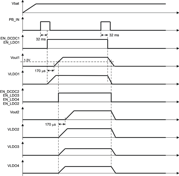 Figure 17. Example Power-up Timing
9.2.2.5 RESET
The TPS65051, TPS65052, TPS65054, and TPS65056 devices contain a comparator that is used to supervise a voltage connected to an external voltage divider, and generate a reset signal if the voltage is lower than the threshold. The rising edge is delayed by 100 ms at the open-drain RESET output. The values for the external resistors R13 to R15 are calculated as follows:
- VL = 3.3 V
- VH = 3.4 V
Set R15 = 100 kΩ
→ R13 + R14 = 240 kΩ
→ R14 = 3.03 kΩ
→ R13 = 237 kΩ
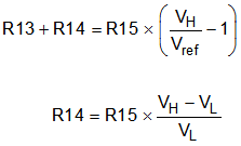
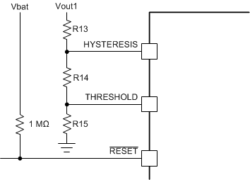 Figure 18. RESET Circuit
9.2.3 Application Curves
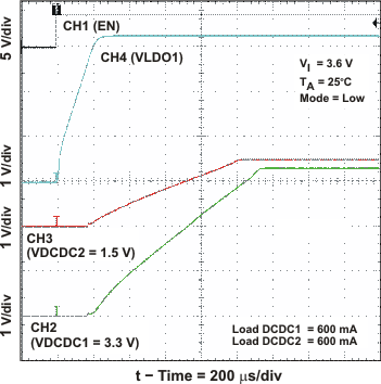 Figure 21. DCDC1 Start-up Timing
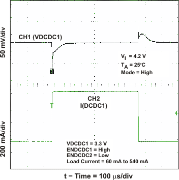 Figure 23. DCDC1 Load Transient Response
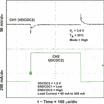 Figure 25. DCDC2 Load Transient Response
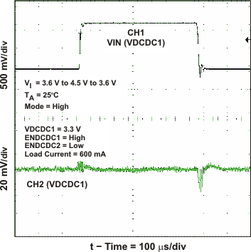 Figure 27. DCDC1 Line Transient Response
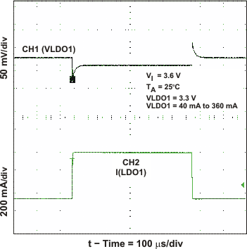 Figure 29. LDO1 Load Transient Response
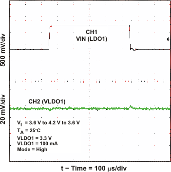
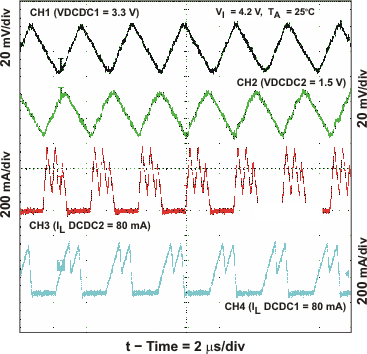
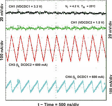 Figure 20. Output Voltage Ripple PWM Mode = HIGH
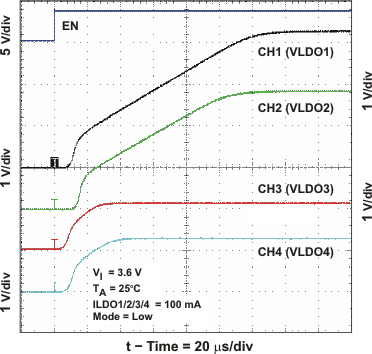 Figure 22. LDO1 to LDO4 Start-up Timing
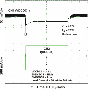 Figure 24. DCDC1 Load Transient Response
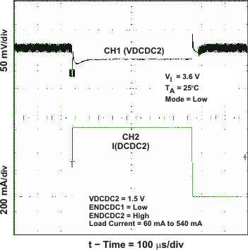 Figure 26. DCDC2 Load Transient Response
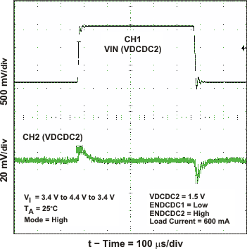 Figure 28. DCDC2 Line Transient Response
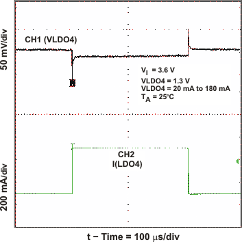 Figure 30. LDO4 Load Transient Response
