SLVS949F May 2009 – May 2017 TPS54620
PRODUCTION DATA.
- 1 Features
- 2 Applications
- 3 Description
- 4 Revision History
- 5 Pin Configurations and Functions
- 6 Specifications
-
7 Detailed Description
- 7.1 Overview
- 7.2 Functional Block Diagram
- 7.3
Feature Description
- 7.3.1 Fixed Frequency PWM Control
- 7.3.2 Continuous Current Mode Operation (CCM)
- 7.3.3 VIN and Power VIN Pins (VIN and PVIN)
- 7.3.4 Voltage Reference
- 7.3.5 Adjusting the Output Voltage
- 7.3.6 Safe Start-Up into Prebiased Outputs
- 7.3.7 Error Amplifier
- 7.3.8 Slope Compensation
- 7.3.9 Enable and Adjusting Undervoltage Lockout
- 7.3.10 Adjustable Switching Frequency and Synchronization (RT/CLK)
- 7.3.11 Slow Start (SS/TR)
- 7.3.12 Power Good (PWRGD)
- 7.3.13 Output Overvoltage Protection (OVP)
- 7.3.14 Overcurrent Protection
- 7.3.15 Thermal Shutdown
- 7.3.16 Small Signal Model for Loop Response
- 7.3.17 Simple Small Signal Model for Peak Current Mode Control
- 7.3.18 Small Signal Model for Frequency Compensation
- 7.4 Device Functional Modes
-
8 Application and Implementation
- 8.1 Application Information
- 8.2
Typical Application
- 8.2.1 Design Requirements
- 8.2.2
Detailed Design Procedures
- 8.2.2.1 Custom Design With WEBENCH Tools
- 8.2.2.2 Operating Frequency
- 8.2.2.3 Output Inductor Selection
- 8.2.2.4 Output Capacitor Selection
- 8.2.2.5 Input Capacitor Selection
- 8.2.2.6 Slow-Start Capacitor Selection
- 8.2.2.7 Bootstrap Capacitor Selection
- 8.2.2.8 Undervoltage Lockout Set Point
- 8.2.2.9 Output Voltage Feedback Resistor Selection
- 8.2.2.10 Compensation Component Selection
- 8.2.2.11 Fast Transient Considerations
- 8.2.3 Application Curves
- 9 Power Supply Recommendations
- 10Layout
- 11Device and Documentation Support
- 12Mechanical, Packaging, and Orderable Information
10 Layout
10.1 Layout Guidelines
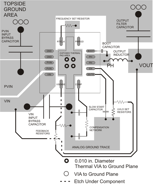
- Layout is a critical portion of good power supply design. See Figure 55 for a PCB layout example.
- The top layer contains the main power traces for VIN, VOUT, and VPHASE. Also, on the top layer are connections for the remaining pins of the TPS54620 and a large top-side area filled with ground.
- The top layer ground area must be connected to the internal ground layer(s) using vias at the input bypass capacitor, the output filter capacitor and directly under the TPS54620 device to provide a thermal path from the exposed thermal pad land to ground.
- The GND pin must be tied directly to the power pad under the IC and the power pad.
- For operation at full rated load, the top side ground area together with the internal ground plane, must provide adequate heat dissipating area.
- There are several signals paths that conduct fast changing currents or voltages that can interact with stray inductance or parasitic capacitance to generate noise or degrade the power supplies performance.
- To help eliminate these problems, the PVIN pin must be bypassed to ground with a low ESR ceramic bypass capacitor with X5R or X7R dielectric.
- Take care to minimize the loop area formed by the bypass capacitor connections, the PVIN pins, and the ground connections.
- The VIN pin must also be bypassed to ground using a low ESR ceramic capacitor with X5R or X7R dielectric.
- Make sure to connect this capacitor to the quite analog ground trace rather than the power ground trace of the PVIn bypass capacitor.
- Since the PH connection is the switching node, the output inductor must be placed close to the PH pins, and the area of the PCB conductor minimized to prevent excessive capacitive coupling.
- The output filter capacitor ground must use the same power ground trace as the PVIN input bypass capacitor.
- Try to minimize this conductor length while maintaining adequate width.
- The small signal components must be grounded to the analog ground path as shown.
- All sensitive analog traces and components such as VSENSE, RT/CLK and COMP must be placed away from high-voltage switching nodes such as PH, BOOT and the output inductor to avoid noise coupling.
- The output voltage sense trace must be connected to the positive terminal of one output capacitor in the design, with the best high frequency characteristics. The output voltage will be most tightly regulated at the voltage sense point.
- The RT/CLK pin is sensitive to noise so the RT resistor must be placed as close as possible to the IC and routed with minimal lengths of trace.
- The additional external components can be placed approximately as shown.
- It may be possible to obtain acceptable performance with alternate PCB layouts, however this layout has been shown to produce good results and is meant as a guideline.
- Land pattern and stencil information is provided in the data sheet addendum.
- The dimension and outline information is for the standard RHL (S-PVQFN-N14) package.
- There may be slight differences between the provided data and actual lead frame used on the TPS54620RGY package. The RGY package is identical to the RHL package. The RHL footprint should be used for both packages.
10.2 Layout Example
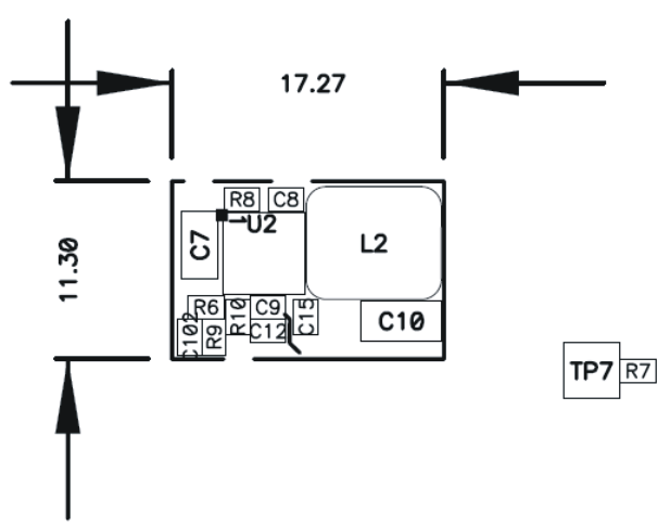
 Figure 56. Ultra-Small PCB Layout Using TPS54620 (PMP4854-2)
10.3 Estimated Circuit Area
The estimated printed-circuit board area for the components used in the design of Figure 34 is 0.58. in2 (374 mm2). This area does not include test points or connectors.
The board area can be further reduced if size is a big concern in an application. Figure 56 shows the printed circuit board layout for PMP4854-2 as shown in Figure 35 whose board area is as small as 17.27 mm × 11.30 mm.
10.4 Thermal Consideration
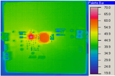
 Figure 57. Thermal Signature of TPS54620EVM-374 Operating at
 VIN = 12 V, VOUT = 3.3 V, 6 A, TA = Room Temperature
