SLVS950I July 2009 – May 2018 TPS65070 , TPS65072 , TPS65073 , TPS650731 , TPS650732
UNLESS OTHERWISE NOTED, this document contains PRODUCTION DATA.
- 1 Features
- 2 Applications
- 3 Description
- 4 Revision History
- 5 Description (continued)
- 6 Device Options
- 7 Pin Configuration and Functions
-
8 Specifications
- 8.1 Absolute Maximum Ratings
- 8.2 ESD Ratings
- 8.3 Recommended Operating Conditions
- 8.4 Thermal Information
- 8.5 Electrical Characteristics
- 8.6 Electrical Characteristics - DCDC1 Converter
- 8.7 Electrical Characteristics - DCDC2 Converter
- 8.8 Electrical Characteristics - DCDC3 Converter
- 8.9 Electrical Characteristics - VLDO1 and VLDO2 Low Dropout Regulators
- 8.10 Electrical Characteristics - wLED Boost Converter
- 8.11 Electrical Characteristics - Reset, PB_IN, PB_OUT, PGood, Power_on, INT, EN_EXTLDO, EN_wLED
- 8.12 Electrical Characteristics - ADC Converter
- 8.13 Electrical Characteristics - Touch Screen Interface
- 8.14 Electrical Characteristics - Power Path
- 8.15 Electrical Characteristics - Battery Charger
- 8.16 Timing Requirements
- 8.17 Dissipation Ratings
- 8.18 Typical Characteristics
- 9 Parameter Measurement Information
-
10Detailed Description
- 10.1 Overview
- 10.2 Functional Block Diagram
- 10.3
Feature Description
- 10.3.1 Battery Charger and Power Path
- 10.3.2 Power Down
- 10.3.3 Power-On Reset
- 10.3.4 Power-Path Management
- 10.3.5 Battery Charging
- 10.3.6 Battery Pack Temperature Monitoring
- 10.3.7 Battery Charger State Diagram
- 10.3.8 DC-DC Converters and LDOs
- 10.3.9 Power Save Mode
- 10.3.10 Short-Circuit Protection
- 10.3.11 Enable
- 10.3.12 Short-Circuit Protection
- 10.3.13 Thermal Shutdown
- 10.4 Device Functional Modes
- 10.5 Programming
- 10.6
Register Maps
- 10.6.1 PPATH1. Register Address: 01h
- 10.6.2 INT. Register Address: 02h
- 10.6.3 CHGCONFIG0. Register Address: 03h
- 10.6.4 CHGCONFIG1. Register Address: 04h
- 10.6.5 CHGCONFIG2. Register Address: 05h
- 10.6.6 CHGCONFIG3. Register Address: 06h
- 10.6.7 ADCONFIG. Register Address: 07h
- 10.6.8 TSCMODE. Register Address: 08h
- 10.6.9 ADRESULT_1. Register Address: 09h
- 10.6.10 ADRESULT_2. Register Address: 0Ah
- 10.6.11 PGOOD. Register Address: 0Bh
- 10.6.12 PGOODMASK. Register Address: 0Ch
- 10.6.13 CON_CTRL1. Register Address: 0Dh
- 10.6.14 CON_CTRL2. Register Address: 0Eh
- 10.6.15 CON_CTRL3. Register Address: 0Fh
- 10.6.16 DEFDCDC1. Register Address: 10h
- 10.6.17 DEFDCDC2_LOW. Register Address: 11h
- 10.6.18 DEFDCDC2_HIGH. Register Address: 12h
- 10.6.19 DEFDCDC3_LOW. Register Address: 13h
- 10.6.20 DEFDCDC3_HIGH. Register Address: 14h
- 10.6.21 DEFSLEW. Register Address: 15h
- 10.6.22 LDO_CTRL1. Register Address: 16h
- 10.6.23 DEFLDO2. Register Address: 17h
- 10.6.24 WLED_CTRL1. Register Address: 18h
- 10.6.25 WLED_CTRL2. Register Address: 19h
-
11Application and Implementation
- 11.1 Application Information
- 11.2
Typical Applications
- 11.2.1 General PMIC Application
- 11.2.2 Powering OMAP-L138
- 11.2.3 Powering Atlas IV
- 11.2.4 OMAP35xx (Supporting SYS-OFF Mode)
- 11.2.5 TPS650731 for OMAP35xx
- 11.2.6 Powering AM3505 Using TPS650732
- 12Power Supply Recommendations
- 13Layout
- 14Device and Documentation Support
- 15Mechanical, Packaging, and Orderable Information
10.3.5 Battery Charging
When Bit CHARGER ENABLE in register CHGCONFIG1 is set to 1, battery charging can begin. First, the device checks for a short-circuit on the BAT pin: IBAT(SC) is turned on till the voltage on the BAT pin rises above VBAT(SC). If conditions are safe, it proceeds to charge the battery.
The battery is charged in three phases: conditioning precharge, constant current fast charge (current regulation) and a constant voltage tapering-off (voltage regulation). In all charge phases, an internal control loop monitors the IC junction temperature and reduces the charge current if the internal temperature threshold is exceeded.
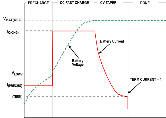
Figure 28 shows what happens in each of the three phases.
 Figure 28. Battery Charge
In the precharge phase, the battery is charged at a current of IPRECHG. The battery voltage starts rising. Once the battery voltage crosses the VLOWV threshold, the battery is charged at a current of ICHG. The battery voltage continues to rise. When the battery voltage reaches VBAT(REG), the battery is held at a constant value of VBAT(REG). The battery current now decreases as the battery approaches full charge. When the battery current reaches ITERM, the TERM CURRENT flag in register CHGCONFIG0 indicates charging done by going high.
Note that termination detection is disabled whenever the charge rate is reduced from the set point because of the actions of the thermal loop, the DPM loop or the VIN-LOW loop.
The value of the fast-charge current is set by the resistor connected from the ISET pin to GND, and is given by the equation
Note that if ICHG is programmed as greater than the input current limit, the battery will not charge at the rate of ICHG, but at the slower rate of IIN-MAX (minus the load current on the OUT pin, if any). In this case, the charger timers will be slowed down by 2x whenever the thermal loop or DPPM is active.