SLVSA92C November 2011 – September 2020 TPS63060 , TPS63061
PRODUCTION DATA
- 1 Features
- 2 Applications
- 3 Description
- 4 Revision History
- 5 Device Comparison
- 6 Pin Configuration and Functions
- 7 Specifications
- 8 Detailed Description
- 9 Application and Implementation
- 10Power Supply Recommendations
- 11Layout
- 12Device and Documentation Support
- 13Mechanical, Packaging, and Orderable Information
8.4.2 Control Loop
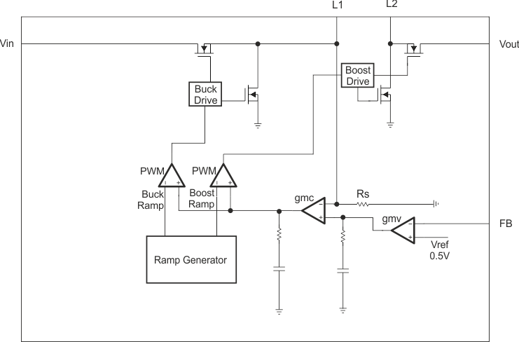
The controller circuit of the device is based on an average current mode topology. The average inductor current is regulated by a fast current regulator loop which is controlled by a voltage control loop. Figure 8-3 shows the control loop.
 Figure 8-3 Average Current Mode Control
The non inverting input of the transconductance amplifier, gMV, is assumed to be constant. The output of gMV defines the average inductor current. The inductor current is reconstructed by measuring the current through the high side buck MOSFET. This current corresponds exactly to the inductor current in boost mode. In buck mode the current is measured during the on time of the same MOSFET. During the off time, the current is reconstructed internally starting from the peak value at the end of the on-time cycle. The average current is compared to the desired value and the difference, or current error, is amplified and compared to the buck or the boost sawtooth ramp. Depending on which of the two ramps the gMC amplified output crosses, the device acitvates either the buck MOSFETs or the boost MOSFETs. When the input voltage is close to the output voltage, one boost cycle always follows a buck cycle. In this condition, no more than three cycles in a row of the same mode are allowed. This control method in the buck-boost region ensures a robust control and the highest efficiency.