SLVSAA4G June 2010 – February 2018 TPS65251
PRODUCTION DATA.
- 1 Features
- 2 Applications
- 3 Description
- 4 Revision History
- 5 Description (continued)
- 6 Pin Configuration and Functions
- 7 Specifications
-
8 Detailed Description
- 8.1 Overview
- 8.2 Functional Block Diagram
- 8.3
Feature Description
- 8.3.1 Adjustable Switching Frequency
- 8.3.2 Synchronization
- 8.3.3 Out-of-Phase Operation
- 8.3.4 Delayed Start-Up
- 8.3.5 Soft-Start Time
- 8.3.6 Adjusting the Output Voltage
- 8.3.7 Input Capacitor
- 8.3.8 Bootstrap Capacitor
- 8.3.9 Error Amplifier
- 8.3.10 Loop Compensation
- 8.3.11 Slope Compensation
- 8.3.12 Powergood
- 8.3.13 Current Limit Protection
- 8.3.14 Overvoltage Transient Protection
- 8.3.15 Thermal Shutdown
- 8.4 Device Functional Modes
-
9 Application and Implementation
- 9.1 Application Information
- 9.2
Typical Application
- 9.2.1 Design Requirements
- 9.2.2
Detailed Design Procedure
- 9.2.2.1 Loop Compensation Circuit
- 9.2.2.2 Selecting the Switching Frequency
- 9.2.2.3 Output Inductor Selection
- 9.2.2.4 Output Capacitor
- 9.2.2.5 Input Capacitor
- 9.2.2.6 Soft-Start Capacitor
- 9.2.2.7 Bootstrap Capacitor Selection
- 9.2.2.8 Adjustable Current Limiting Resistor Selection
- 9.2.2.9 Output Voltage and Feedback Resistors Selection
- 9.2.2.10 Compensation
- 9.2.2.11 3.3-V and 6.5-V LDO Regulators
- 9.2.3 Application Curves
- 10Power Supply Recommendations
- 11Layout
- 12Device and Documentation Support
- 13Mechanical, Packaging, and Orderable Information
8.3.13 Current Limit Protection
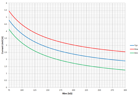
Figure 17 shows the (peak) inductor current limit for Buck 1. The typical limit can be approximated with the following graph.
 Figure 17. Buck 1
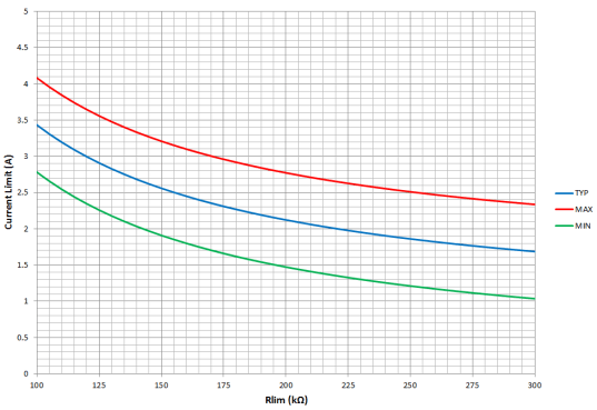
Figure 18 shows the (peak) inductor current limit for Buck 2. The typical limit can be approximated with the following graph.
 Figure 18. Buck 2
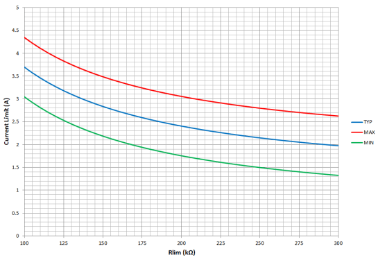
Figure 19 shows the (peak) inductor current limit for Buck 3. The typical limit can be approximated with the following graph.
 Figure 19. Buck 3
All converters operate in hiccup mode: Once an over-current lasting more than 10 ms is sensed in any of the converters, all the converters will shut down for 10 ms and then the start-up sequencing will be tried again. If the overload has been removed, the converter will ramp up and operate normally. If this is not the case the converter will see another over-current event and shuts-down again repeating the cycle (hiccup) until the failure is cleared.
If an overload condition lasts for less than 10 ms, only the relevant converter affected will go into and out of under-voltage and no global hiccup mode will occur. The converter will be protected by the cycle-by-cycle current limit during that time.