SLVSAL5E November   2011  – October 2021 TPS62150 , TPS62150A , TPS62151 , TPS62152 , TPS62153

PRODUCTION DATA  

  1. Features
  2. Applications
  3. Description
  4. Revision History
  5. Device Comparison Table
  6. Pin Configuration and Functions
  7. Specifications
    1. 7.1 Absolute Maximum Ratings (1)
    2. 7.2 ESD Ratings
    3. 7.3 Recommended Operating Conditions
    4. 7.4 Thermal Information
    5. 7.5 Electrical Characteristics
    6. 7.6 Typical Characteristics
  8. Detailed Description
    1. 8.1 Overview
    2. 8.2 Functional Block Diagrams
    3. 8.3 Feature Description
      1. 8.3.1 Enable / Shutdown (EN)
      2. 8.3.2 Soft Start or Tracking (SS/TR)
      3. 8.3.3 Power Good (PG)
      4. 8.3.4 Pin-Selectable Output Voltage (DEF)
      5. 8.3.5 Frequency Selection (FSW)
      6. 8.3.6 Undervoltage Lockout (UVLO)
      7. 8.3.7 Thermal Shutdown
    4. 8.4 Device Functional Modes
      1. 8.4.1 Pulse-Width Modulation (PWM) Operation
      2. 8.4.2 Power-Save Mode Operation
      3. 8.4.3 100% Duty-Cycle Operation
      4. 8.4.4 Current-Limit and Short-Circuit Protection
  9. Application and Implementation
    1. 9.1 Application Information
    2. 9.2 Typical Application
      1. 9.2.1 Design Requirements
      2. 9.2.2 Detailed Design Procedure
        1. 9.2.2.1 Programming the Output Voltage
        2. 9.2.2.2 External Component Selection
          1. 9.2.2.2.1 Inductor Selection
          2. 9.2.2.2.2 Capacitor Selection
            1. 9.2.2.2.2.1 Output Capacitor
            2. 9.2.2.2.2.2 Input Capacitor
            3. 9.2.2.2.2.3 Soft-Start Capacitor
        3. 9.2.2.3 Tracking Function
        4. 9.2.2.4 Output Filter and Loop Stability
      3. 9.2.3 Application Curves
    3. 9.3 System Examples
      1. 9.3.1 LED Power Supply
      2. 9.3.2 Active Output Discharge
      3. 9.3.3 Inverting Power Supply
      4. 9.3.4 Various Output Voltages
  10. 10Power Supply Recommendations
  11. 11Layout
    1. 11.1 Layout Guidelines
    2. 11.2 Layout Example
      1. 11.2.1 Thermal Considerations
  12. 12Device and Documentation Support
    1. 12.1 Device Support
      1. 12.1.1 Third-Party Products Disclaimer
    2. 12.2 Documentation Support
      1. 12.2.1 Related Documentation
    3. 12.3 Receiving Notification of Documentation Updates
    4. 12.4 Support Resources
    5. 12.5 Trademarks
    6. 12.6 Electrostatic Discharge Caution
    7. 12.7 Glossary
  13. 13Mechanical, Packaging, and Orderable Information

Description

The TPS6215x family is an easy-to-use synchronous step down dc-dc converter optimized for applications with high power density. A high switching frequency of typically 2.5 MHz allows the use of small inductors and provides fast transient response as well as high output-voltage accuracy by the use of DCS-Control topology.

With their wide operating input-voltage range of 3 V to 17 V, the devices are ideally suited for systems powered from either Li-Ion or other batteries as well as from 12-V intermediate power rails. The devices support up to 1-A continuous output current at output voltages between 0.9 V and 6 V (in 100% duty-cycle mode). The soft-start pin controls the output-voltage start-up ramp, which allows operation as either a standalone power supply or in tracking configurations. Power sequencing is also possible by configuring the enable (EN) and open-drain power-good (PG) pins.

In power-save mode, the devices draw quiescent current of about 17 μA from VIN. Power-save-mode, entered automatically and seamlessly if the load is small, maintains high efficiency over the entire load range. In shutdown mode, the device turns off and current consumption is less than 2 μA.

The device, available in adjustable- and fixed-output-voltage versions, comes in a 16-pin VQFN package measuring 3 × 3 mm (RGT).

Device Information
PART NUMBERPACKAGE(1)BODY SIZE (NOM)
TPS6215XVQFN (16)3.00 mm × 3.00 mm
For all available packages, see the orderable addendum at the end of the data sheet.
GUID-6124CEDE-720D-430B-BE33-D02897A6B4BC-low.gifTypical Application Schematic
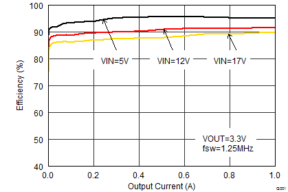
GUID-E6C0DA5E-4C2D-4F0D-A200-95E87C36036C-low.pngEfficiency vs Output Current