SLVSAX7E August 2011 – August 2016 TPS65270
PRODUCTION DATA.
- 1 Features
- 2 Applications
- 3 Description
- 4 Revision History
- 5 Description (continued)
- 6 Pin Configuration and Functions
- 7 Specifications
- 8 Detailed Description
- 9 Application and Implementation
- 10Power Supply Recommendations
- 11Layout
- 12Device and Documentation Support
- 13Mechanical, Packaging, and Orderable Information
9 Application and Implementation
NOTE
Information in the following applications sections is not part of the TI component specification, and TI does not warrant its accuracy or completeness. TI’s customers are responsible for determining suitability of components for their purposes. Customers should validate and test their design implementation to confirm system functionality.
9.1 Application Information
The device is a dual-synchronous, step-down DC-DC converter. It is typically used to convert a higher DC voltage to lower DC voltages with continuous available output current of 2 A or 3 A.
9.2 Typical Application
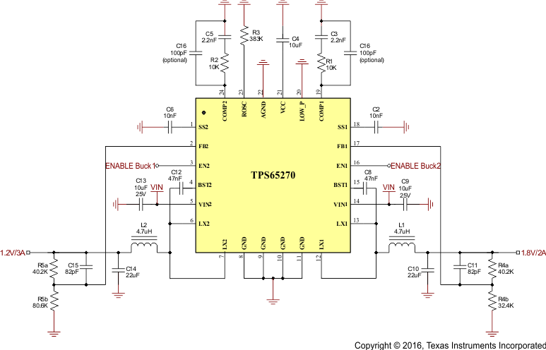 Figure 9. Typical Application Schematic
9.2.1 Design Requirements
For this design example, use the parameters listed in Table 1 as the input parameters.
Table 1. Design Parameters
| PARAMETER | EXAMPLE VALUE |
|---|---|
| VOUT1 | 1.8 V |
| IOUT1 | 2 A |
| VOUT2 | 1.2 V |
| IOUT2 | 3 A |
| Transient response (1-A load step) | ±5% |
| Input voltage | 12 V (typical), 4.5 V to 18 V |
| Output voltage ripple | ±1% |
| Switching frequency | 625 kHz |
9.2.2 Detailed Design Procedure
9.2.2.1 Output Inductor Selection
To calculate the value of the output inductor, use Equation 4. LIR is a coefficient that represents the amount of inductor ripple current relative to the maximum output current. The inductor ripple current is filtered by the output capacitor. Therefore, choosing high inductor ripple currents impact the selection of the output capacitor since the output capacitor must have a ripple current rating equal to or greater than the inductor ripple current. In general, the inductor ripple value is at the discretion of the designer; however, LIR is normally from 0.1 to 0.3 for the majority of applications.

For the output filter inductor, it is important that the RMS current and saturation current ratings not be exceeded. The RMS and peak inductor current can be found from Equation 6 and Equation 7.


The current flowing through the inductor is the inductor ripple current plus the output current. During power up, faults or transient load conditions, the inductor current can increase above the calculated peak inductor current level calculated above. In transient conditions, the inductor current can increase up to the switch current limit of the device. For this reason, the most conservative approach is to specify an inductor with a saturation current rating equal to or greater than the switch current limit rather than the peak inductor current.
9.2.2.2 Output Capacitor Selection
There are three primary considerations for selecting the value of the output capacitor. The output capacitor determines the modulator pole, the output voltage ripple, and how the regulator responds to a large change in load current. The output capacitance needs to be selected based on the most stringent of these three criteria.
The desired response to a large change in the load current is the first criteria. The output capacitor needs to supply the load with current when the regulator cannot. This situation would occur if there are desired hold-up times for the regulator where the output capacitor must hold the output voltage above a certain level for a specified amount of time after the input power is removed. The regulator is also temporarily not able to supply sufficient output current if there is a large, fast increase in the current needs of the load such as a transition from no load to full load. The regulator usually needs two or more clock cycles for the control loop to see the change in load current and output voltage and adjust the duty cycle to react to the change. The output capacitor must be sized to supply the extra current to the load until the control loop responds to the load change. The output capacitance must be large enough to supply the difference in current for 2 clock cycles while only allowing a tolerable amount of droop in the output voltage. Equation 8 shows the minimum output capacitance necessary to accomplish this.

where
- ΔIout is the change in output current
- ƒsw is the regulators switching frequency
- ΔVout is the allowable change in the output voltage.
Equation 9 calculates the minimum output capacitance needed to meet the output voltage ripple specification.

where
- ƒsw is the switching frequency.
- Vripple is the maximum allowable output voltage ripple.
- Iripple is the inductor ripple current.
Equation 10 calculates the maximum ESR an output capacitor can have to meet the output voltage ripple specification.

Additional capacitance deratings for aging, temperature and DC bias should be factored in which increases this minimum value. Capacitors generally have limits to the amount of ripple current they can handle without failing or producing excess heat. An output capacitor that can support the inductor ripple current must be specified. Some capacitor data sheets specify the root mean square (RMS) value of the maximum ripple current. Equation 11 can be used to calculate the RMS ripple current the output capacitor needs to support.

9.2.2.3 Input Capacitor Selection
The TPS65265 requires a high quality ceramic, type X5R or X7R, input decoupling capacitor of at least 10 µF of effective capacitance on the PVIN input voltage pins. These capacitors must be connected as close as physically possible to the input pins of the converters. In some applications additional bulk capacitance may also be required for the PVIN input. The effective capacitance includes any DC bias effects. The voltage rating of the input capacitor must be greater than the maximum input voltage. The capacitor must also have a ripple current rating greater than the maximum input current ripple of The TPS65265. The input ripple current can be calculated using Equation 12.

The value of a ceramic capacitor varies significantly over temperature and the amount of DC bias applied to the capacitor. The capacitance variations due to temperature can be minimized by selecting a dielectric material that is stable over temperature. X5R and X7R ceramic dielectrics are usually selected for power regulator capacitors because they have a high capacitance to volume ratio and are fairly stable over temperature. The output capacitor must also be selected with the DC bias taken into account. The capacitance value of a capacitor decreases as the DC bias across a capacitor increases. The input capacitance value determines the input ripple voltage of the regulator. The input voltage ripple can be calculated using Equation 13.

9.2.2.4 Bootstrap Capacitor Selection
The device has two integrated boot regulators and requires a small ceramic capacitor between BST and LX pins to provide the gate drive voltage for the high side MOSFET. TI recommends a ceramic capacitor of 0.047 µF. A ceramic capacitor with an X7R or X5R grade dielectric is desired because of the stable characteristics over temperature and voltage.
9.2.2.5 Loop Compensation
TPS65270 is a current mode control DC-DC converter. The error amplifier has 130-µA/V transconductance.
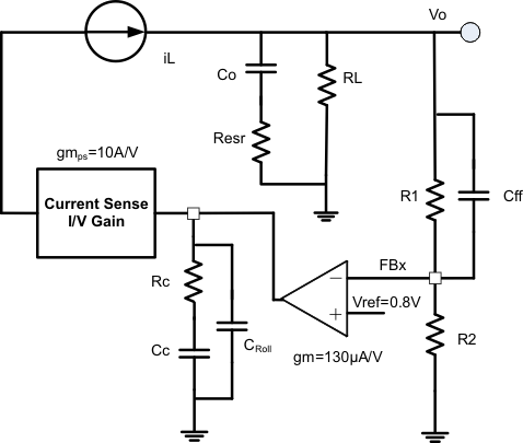 Figure 10. Loop Compensation
A typical compensation circuit could be type II (RC and CC) to have a phase margin from 60 to 90 degrees, or type III (RC, CC and Cff) to improve the converter transient response. CRoll adds a high frequency pole to attenuate high-frequency noise when required. It may also prevent noise coupling from other rails if there is possibility of cross coupling between rails when layout is very compact.
To calculate the external compensation components follow the following steps:
| TYPE II CIRCUIT | TYPE III CIRCUIT | |
|---|---|---|
| Select switching frequency that is appropriate for application depending on L, C sizes, output ripple, EMI concerns and etc. Switching frequencies from 500 kHz to 1 MHz give best trade off between performance and cost. When using smaller L and Cs, switching frequency can be increased. To optimize efficiency, switching frequency can be lowered. | — | Use type III circuit for switching frequencies higher than 500 kHz. |
| Select cross over frequency (fC) to be less than 1/5 to 1/10 of switching frequency. | Suggested fC = fS / 10 | Suggested fC = fS / 10 |
| Set and calculate RC. |
 |
 |
Calculate CC by placing a compensation zero at or before the converter dominant pole  |
 |
 |
Add CRoll if required to remove large signal coupling to high impedance COMP node. Make sure that  |
 |
 |
| Calculate Cff compensation zero at low frequency to boost the phase margin at the crossover frequency. Make sure that the zero frequency (fzff is smaller than soft start equivalent frequency (1 / Tss). | — |
 |
9.2.3 Application Curves
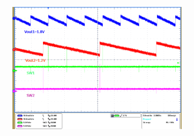
TA = 25°C, VIN = 12 V, fSW = 625 kHz (unless otherwise noted).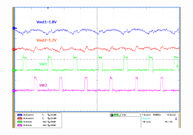
| IO1 = 0 A | IO2 = 0 A |
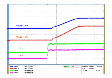
| VO1 = 1.8 V | VO2 = 1.2 V |
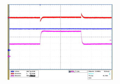
| VO2 = 1 V | IO1 = 1 A to 2 A |
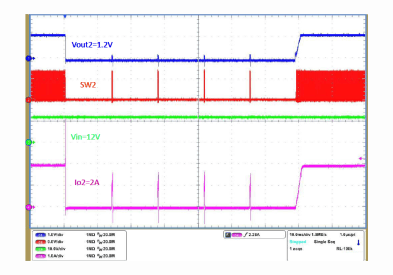 Figure 17. Buck 2 Hard Short and Recover
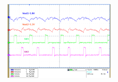
| IO1 = 2 A | IO2 = 3 A |
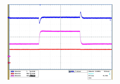
| VO1 = 3.3 V | IO1 = 1 A to 2 A |
