SLVSB09C September 2011 – October 2017 TPS54623
PRODUCTION DATA.
- 1 Features
- 2 Applications
- 3 Description
- 4 Revision History
- 5 Pin Configuration and Functions
- 6 Specifications
-
7 Detailed Description
- 7.1 Overview
- 7.2 Functional Block Diagram
- 7.3
Feature Description
- 7.3.1 VIN and Power VIN Pins (VIN and PVIN)
- 7.3.2 Voltage Reference
- 7.3.3 Adjusting the Output Voltage
- 7.3.4 Safe Start-up into Pre-Biased Outputs
- 7.3.5 Error Amplifier
- 7.3.6 Slope Compensation
- 7.3.7 Enable and Adjusting Undervoltage Lockout
- 7.3.8 Slow Start (SS/TR)
- 7.3.9 Power Good (PWRGD)
- 7.3.10 Bootstrap Voltage (BOOT) and Low Dropout Operation
- 7.3.11 Sequencing (SS/TR)
- 7.3.12 Output Overvoltage Protection (OVP)
- 7.3.13 Overcurrent Protection
- 7.3.14 Thermal Shutdown
- 7.3.15 Small Signal Model for Loop Response
- 7.3.16 Simple Small Signal Model for Peak Current Mode Control
- 7.3.17 Small Signal Model for Frequency Compensation
- 7.4 Device Functional Modes
-
8 Application and Implementation
- 8.1 Application Information
- 8.2
Typical Application
- 8.2.1 Design Requirements
- 8.2.2
Detailed Design Procedure
- 8.2.2.1 Custom Design With WEBENCH® Tools
- 8.2.2.2 Operating Frequency
- 8.2.2.3 Output Inductor Selection
- 8.2.2.4 Output Capacitor Selection
- 8.2.2.5 Input Capacitor Selection
- 8.2.2.6 Slow Start Capacitor Selection
- 8.2.2.7 Bootstrap Capacitor Selection
- 8.2.2.8 Under Voltage Lockout Set Point
- 8.2.2.9 Output Voltage Feedback Resistor Selection
- 8.2.2.10 Compensation Component Selection
- 8.2.3 Application Curves
- 9 Power Supply Recommendations
- 10Layout
- 11Device and Documentation Support
- 12Mechanical, Packaging, and Orderable Information
8 Application and Implementation
NOTE
Information in the following applications sections is not part of the TI component specification, and TI does not warrant its accuracy or completeness. TI’s customers are responsible for determining suitability of components for their purposes. Customers should validate and test their design implementation to confirm system functionality.
8.1 Application Information
8.1.1 Fast Transient Considerations
In applications where fast transient responses are important, Type III frequency compensation can be used instead of the traditional Type II frequency compensation.
For more information about Type II and Type III frequency compensation circuits, see Designing Type III Compensation for Current Mode Step-Down Converters (SLVA352) and Design Calculator (SLVC219).
8.2 Typical Application
 Figure 31. Typical Application Circuit
8.2.1 Design Requirements
This example details the design of a high frequency switching regulator design using ceramic output capacitors. A few parameters must be known in order to start the design process. These parameters are typically determined at the system level. For this example, start with the parameters in Table 1.
Table 1. Design Parameters
| PARAMETER | VALUE |
|---|---|
| Output voltage | 3.3 V |
| Output current | 6 A |
| Transient response 1-A load step | ΔVOUT = 5 % |
| Input voltage | 12 V nominal, 8 V to 17 V |
| Output voltage ripple | 33 mV p-p |
| Start input voltage (rising VIN) | 6.528 V |
| Stop input voltage (falling VIN) | 6.19 V |
| Switching frequency | 480 kHz |
8.2.2 Detailed Design Procedure
8.2.2.1 Custom Design With WEBENCH® Tools
Click here to create a custom design using the TPS54623 device with the WEBENCH® Power Designer.
- Start by entering the input voltage (VIN), output voltage (VOUT), and output current (IOUT) requirements.
- Optimize the design for key parameters such as efficiency, footprint, and cost using the optimizer dial.
- Compare the generated design with other possible solutions from Texas Instruments.
The WEBENCH Power Designer provides a customized schematic along with a list of materials with real-time pricing and component availability.
In most cases, these actions are available:
- Run electrical simulations to see important waveforms and circuit performance
- Run thermal simulations to understand board thermal performance
- Export customized schematic and layout into popular CAD formats
- Print PDF reports for the design, and share the design with colleagues
Get more information about WEBENCH tools at www.ti.com/WEBENCH.
8.2.2.2 Operating Frequency
The first step is to decide on a switching frequency for the regulator. There is a trade off between higher and lower switching frequencies. Higher switching frequencies may produce smaller a solution size using lower valued inductors and smaller output capacitors compared to a power supply that switches at a lower frequency. However, the higher switching frequency causes extra switching losses, which hurt the converter’s efficiency and thermal performance. In this design, a moderate switching frequency of 480 kHz is selected to achieve both a small solution size and a high efficiency operation.
8.2.2.3 Output Inductor Selection
To calculate the value of the output inductor, use Equation 18. KIND is a coefficient that represents the amount of inductor ripple current relative to the maximum output current. The inductor ripple current is filtered by the output capacitor. Therefore, choosing high inductor ripple currents impact the selection of the output capacitor since the output capacitor must have a ripple current rating equal to or greater than the inductor ripple current. In general, the inductor ripple value is at the discretion of the designer; however, KIND is normally from 0.1 to 0.3 for the majority of applications.

For this design example, use KIND = 0.3 and the inductor value is calculated to be 3.08 µH. For this design, a nearest standard value was chosen: 3.3 µH. For the output filter inductor, it is important that the RMS current and saturation current ratings not be exceeded. The RMS and peak inductor current can be found from Equation 20 and Equation 21.


For this design, the RMS inductor current is 6.02 A and the peak inductor current is 6.84 A. The chosen inductor is a Coilcraft MSS1048 series 3.3 µH. It has a saturation current rating of 7.38 A and a RMS current rating of 7.22 A.
The current flowing through the inductor is the inductor ripple current plus the output current. During power up, faults or transient load conditions, the inductor current can increase above the calculated peak inductor current level calculated above. In transient conditions, the inductor current can increase up to the switch current limit of the device. For this reason, the most conservative approach is to specify an inductor with a saturation current rating equal to or greater than the switch current limit rather than the peak inductor current.
8.2.2.4 Output Capacitor Selection
There are three primary considerations for selecting the value of the output capacitor. The output capacitor determines the modulator pole, the output voltage ripple, and how the regulator responds to a large change in load current. The output capacitance needs to be selected based on the more stringent of these three criteria.
The desired response to a large change in the load current is the first criteria. The output capacitor needs to supply the load with current when the regulator can not. This situation would occur if there are desired hold-up times for the regulator where the output capacitor must hold the output voltage above a certain level for a specified amount of time after the input power is removed. The regulator is also temporarily not able to supply sufficient output current if there is a large, fast increase in the current needs of the load such as a transition from no load to full load. The regulator usually needs two or more clock cycles for the control loop to see the change in load current and output voltage and adjust the duty cycle to react to the change. The output capacitor must be sized to supply the extra current to the load until the control loop responds to the load change. The output capacitance must be large enough to supply the difference in current for 2 clock cycles while only allowing a tolerable amount of droop in the output voltage. Equation 22 shows the minimum output capacitance necessary to accomplish this.

Where ΔIout is the change in output current, fsw is the regulators switching frequency and ΔVout is the allowable change in the output voltage. For this example, the transient load response is specified as a 5% change in Vout for a load step of 1 A. For this example, ΔIout = 3.0 A and ΔVout = 0.05 × 3.3 = 0.165 V. Using these numbers gives a minimum capacitance of 75.8 μF. This value does not take the ESR of the output capacitor into account in the output voltage change. For ceramic capacitors, the ESR is usually small enough to ignore in this calculation.
Equation 23 calculates the minimum output capacitance needed to meet the output voltage ripple specification. Where fsw is the switching frequency, Vripple is the maximum allowable output voltage ripple, and Iripple is the inductor ripple current. In this case, the maximum output voltage ripple is 33 mV. Under this requirement, Equation 23 yields 13.2 µF.

Equation 24 calculates the maximum ESR an output capacitor can have to meet the output voltage ripple specification. Equation 24 indicates the ESR should be less than 19.7 mΩ. In this case, the ceramic caps’ ESR is much smaller than 19.7 mΩ.

Additional capacitance de-ratings for aging, temperature and DC bias should be factored in which increases this minimum value. For this example, a 100-μF 6.3-V X5R ceramic capacitor with 3 mΩ of ESR is be used. Capacitors generally have limits to the amount of ripple current they can handle without failing or producing excess heat. An output capacitor that can support the inductor ripple current must be specified. Some capacitor data sheets specify the root mean square (RMS) value of the maximum ripple current. Equation 25 can be used to calculate the RMS ripple current the output capacitor needs to support. For this application, Equation 25 yields 485 mA.

8.2.2.5 Input Capacitor Selection
The TPS54623 requires a high quality ceramic, type X5R or X7R, input decoupling capacitor of at least 4.7 µF of effective capacitance on the PVIN input voltage pins and 4.7 µF on the Vin input voltage pin. In some applications additional bulk capacitance may also be required for the PVIN input. The effective capacitance includes any DC bias effects. The voltage rating of the input capacitor must be greater than the maximum input voltage. The capacitor must also have a ripple current rating greater than the maximum input current ripple of the TPS54623. The input ripple current can be calculated using Equation 26.

The value of a ceramic capacitor varies significantly over temperature and the amount of DC bias applied to the capacitor. The capacitance variations due to temperature can be minimized by selecting a dielectric material that is stable over temperature. X5R and X7R ceramic dielectrics are usually selected for power regulator capacitors because they have a high capacitance to volume ratio and are fairly stable over temperature. The output capacitor must also be selected with the DC bias taken into account. The capacitance value of a capacitor decreases as the DC bias across a capacitor increases. For this example design, a ceramic capacitor with at least a 25 V voltage rating is required to support the maximum input voltage. For this example, one 10 μF and one 4.7 µF 25 V capacitors in parallel have been selected as the VIN and PVIN inputs are tied together so the TPS54623 may operate from a single supply. The input capacitance value determines the input ripple voltage of the regulator. The input voltage ripple can be calculated using Equation 27. Using the design example values, Ioutmax = 6 A, Cin = 14.7 μF, fsw = 480 kHz, yields an input voltage ripple of 213 mV and a RMS input ripple current of 2.95 A.

8.2.2.6 Slow Start Capacitor Selection
The slow start capacitor determines the minimum amount of time it takes for the output voltage to reach its nominal programmed value during power up. This is useful if a load requires a controlled voltage slew rate. This is also used if the output capacitance is very large and would require large amounts of current to quickly charge the capacitor to the output voltage level. The large currents necessary to charge the capacitor may make the TPS54623 reach the current limit or excessive current draw from the input power supply may cause the input voltage rail to sag. Limiting the output voltage slew rate solves both of these problems. The soft start capacitor value can be calculated using Equation 28. For the example circuit, the soft start time is not too critical since the output capacitor value is 100 μF which does not require much current to charge to 3.3 V. The example circuit has the soft start time set to an arbitrary value of 6 ms which requires a 22 nF capacitor. In TPS54623, Iss is 2.3 uA and Vref is 0.6 V.

8.2.2.7 Bootstrap Capacitor Selection
A 0.1-µF ceramic capacitor must be connected between the BOOT to PH pin for proper operation. It is recommended to use a ceramic capacitor with X5R or better grade dielectric. The capacitor should have 10 V or higher voltage rating.
8.2.2.8 Under Voltage Lockout Set Point
The Undervoltage Lockout (UVLO) can be adjusted using the external voltage divider network of R3 and R4. R3 is connected between VIN and the EN pin of the TPS54623 and R4 is connected between EN and GND . The UVLO has two thresholds, one for power up when the input voltage is rising and one for power down or brown outs when the input voltage is falling. For the example design, the supply should turn on and start switching once the input voltage increases above 6.528 V (UVLO start or enable). After the regulator starts switching, it should continue to do so until the input voltage falls below 6.190 V (UVLO stop or disable). Equation 2 and Equation 3 can be used to calculate the values for the upper and lower resistor values. For the stop voltages specified the nearest standard resistor value for R3 is 35.7 kΩ and for R4 is 8.06 kΩ.
8.2.2.9 Output Voltage Feedback Resistor Selection
The resistor divider network R5 and R6 is used to set the output voltage. For the example design, 10 kΩ was selected for R5. Using Equation 29, R6 is calculated as 2.22 kΩ. The nearest standard 1% resistor is 2.21 kΩ.

8.2.2.9.1 Minimum Output Voltage
Due to the internal design of the TPS54623, there is a minimum output voltage limit for any given input voltage. The output voltage can never be lower than the internal voltage reference of 0.6 V. Above 0.6 V, the output voltage may be limited by the minimum controllable on time. The minimum output voltage in this case is given by Equation 30.

where
- Voutmin = minimum achievable output voltage
- Ontimemin = minimum controllable on-time (135 nsec maximum)
- Fsmax = maximum switching frequency including tolerance
- Vinmax = maximum input voltage
- Ioutmin = minimum load current
- RDS1min = minimum high side MOSFET on resistance (36-32 mΩ typical)
- RDS2min = minimum low side MOSFET on resistance (19 mΩ typical)
- RL = series resistance of output inductor
8.2.2.10 Compensation Component Selection
There are several industry techniques used to compensate DC/DC regulators. The method presented here is easy to calculate and yields high phase margins. For most conditions, the regulator has a phase margin between 60 and 90 degrees. The method presented here ignores the effects of the slope compensation that is internal to the TPS54623. Since the slope compensation is ignored, the actual crossover frequency is usually lower than the cross over frequency used in the calculations.
First, the modulator pole, fpmod, and the esr zero, fzmod must be calculated using Equation 31 and Equation 32. For Cout, use a derated value of 75 µF. use Equation 33 and Equation 34 to estimate a starting point for the closed loop crossover frequency fco. Then the required compensation components may be derived. For this design example, fpmod is 3.86 kHz and fzmod is 707.4 kHz. Equation 33 is the geometric mean of the modulator pole and the esr zero and Equation 34 is the geometric mean of the modulator pole and one half the switching frequency. Use a frequency near the lower of these two values as the intended crossover frequency fco. In this case Equation 33 yields 52.2 kHz and Equation 34 yields 30.4 kHz. The lower value is 30.4 kHz. A slightly higher frequency of 30 kHz is chosen as the intended crossover frequency.


Now the compensation components can be calculated. First calculate the value for R2 which sets the gain of the compensated network at the crossover frequency. Use Equation 35 to determine the value of R2.

Next calculate the value of C3. Together with R2, C3 places a compensation zero at the modulator pole frequency. Equation 36 to determine the value of C3.

Using Equation 35 and Equation 36 the standard values for R4 and C4 are 3.74 kΩ and 0.01 µF.
An additional high frequency pole can be used if necessary by adding a capacitor in parallel with the series combination of R4 and C4. The pole frequency can be placed at the ESR zero frequency of the output capacitor as given by Equation 12. Use Equation 37 to calculate the required capacitor value for C5.

8.2.3 Application Curves
 Figure 32. Load Transient
 Figure 34. Startup with EN
 Figure 36. Output Voltage Ripple With Full Load
 Figure 38. Closed Loop Response
 Figure 40. Load Regulation
 Figure 42. Maximum Ambient Temperature
vs Load Current
 Figure 44. Junction Temperature
vs IC Power Dissipation
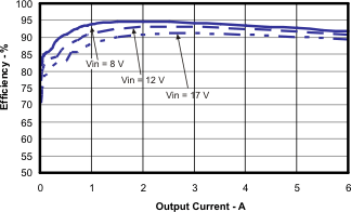
 Figure 46. Efficiency vs Output Current
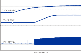
 Figure 33. Start-Up With VIN
 Figure 35. Start-Up With Pre-Bias
 Figure 37. Input Voltage Ripple with Full Load
 Figure 39. Line Regulation
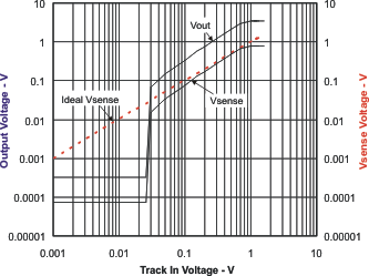
 Figure 41. Tracking Performance
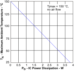
 Figure 43. Maximum Ambient Temperature
vs IC Power Dissipation
 Figure 45. Efficiency vs Load Current
