SLVSB71E February   2012  – September 2016 TLV62150 , TLV62150A

PRODUCTION DATA.  

  1. Features
  2. Applications
  3. Description
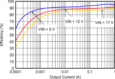
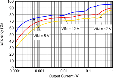
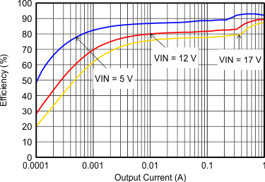
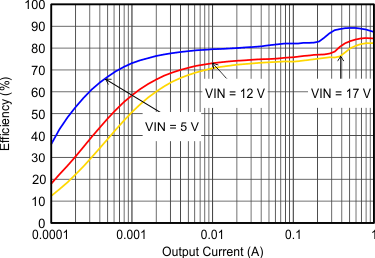
    1.     Device Images
      1.      Typical Application Schematic
      2.      Efficiency vs Output Current
  4. Revision History
  5. Device Comparison Table
  6. Pin Configuration and Functions
    1.     Pin Functions
  7. Specifications
    1. 7.1 Absolute Maximum Ratings
    2. 7.2 ESD Ratings
    3. 7.3 Recommended Operating Conditions
    4. 7.4 Thermal Information
    5. 7.5 Electrical Characteristics
    6. 7.6 Typical Characteristics
  8. Detailed Description
    1. 8.1 Overview
    2. 8.2 Functional Block Diagram
    3. 8.3 Feature Description
      1. 8.3.1 Enable / Shutdown (EN)
      2. 8.3.2 Soft Start / Tracking (SS/TR)
      3. 8.3.3 Power Good (PG)
      4. 8.3.4 Pin-Selectable Output Voltage (DEF)
      5. 8.3.5 Frequency Selection (FSW)
      6. 8.3.6 Undervoltage Lockout (UVLO)
      7. 8.3.7 Thermal Shutdown
    4. 8.4 Device Functional Modes
      1. 8.4.1 Pulse Width Modulation (PWM) Operation
      2. 8.4.2 Power Save Mode Operation
      3. 8.4.3 100% Duty-Cycle Operation
      4. 8.4.4 Current Limit and Short Circuit Protection
  9. Application and Implementation
    1. 9.1 Application Information
    2. 9.2 Typical Application
      1. 9.2.1 Design Requirements
      2. 9.2.2 Detailed Design Procedure
        1. 9.2.2.1 Programming the Output Voltage
        2. 9.2.2.2 External Component Selection
          1. 9.2.2.2.1 Inductor Selection
          2. 9.2.2.2.2 Capacitor Selection
            1. 9.2.2.2.2.1 Output Capacitor
            2. 9.2.2.2.2.2 Input Capacitor
            3. 9.2.2.2.2.3 Soft-Start Capacitor
        3. 9.2.2.3 Tracking Function
        4. 9.2.2.4 Output Filter and Loop Stability
      3. 9.2.3 Application Curves
    3. 9.3 System Examples
      1. 9.3.1 LED Power Supply
      2. 9.3.2 Active Output Discharge
      3. 9.3.3 Inverting Power Supply
      4. 9.3.4 Various Output Voltages
  10. 10Power Supply Recommendations
  11. 11Layout
    1. 11.1 Layout Guidelines
    2. 11.2 Layout Example
    3. 11.3 Thermal Considerations
  12. 12Device and Documentation Support
    1. 12.1 Device Support
      1. 12.1.1 Third-Party Products Disclaimer
    2. 12.2 Related Links
    3. 12.3 Documentation Support
      1. 12.3.1 Related Documentation
    4. 12.4 Receiving Notification of Documentation Updates
    5. 12.5 Community Resources
    6. 12.6 Trademarks
    7. 12.7 Electrostatic Discharge Caution
    8. 12.8 Glossary
  13. 13Mechanical, Packaging, and Orderable Information

Application Curves

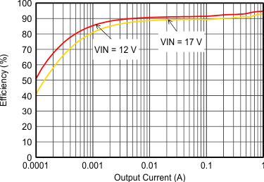
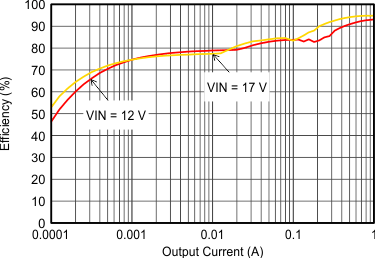
VIN = 12 V, VOUT = 3.3 V, TA = 25°C, (unless otherwise noted)
TLV62150 TLV62150A SLVSAL5_eff50iouthalf.gif
Figure 8. Efficiency With 1.25 MHz, Vout = 5 V
TLV62150 TLV62150A SLVSAL5_eff50ioutfull.gif
Figure 10. Efficiency With 2.5 MHz, Vout = 5 V
TLV62150 TLV62150A SLVSAL5_eff33iouthalf.gif
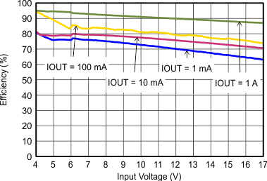
Figure 12. Efficiency With 1.25 MHz, Vout = 3.3 V
TLV62150 TLV62150A SLVSAL5_eff33ioutfull.gif
Figure 14. Efficiency With 2.5 MHz, Vout = 3.3 V
TLV62150 TLV62150A SLVSAL5_eff18iouthalf.gif
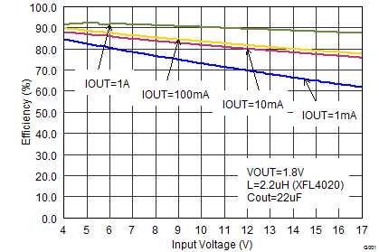
Figure 16. Efficiency With 1.25 MHz, Vout = 1.8 V
TLV62150 TLV62150A SLVSAL5_eff09iouthalf.gif
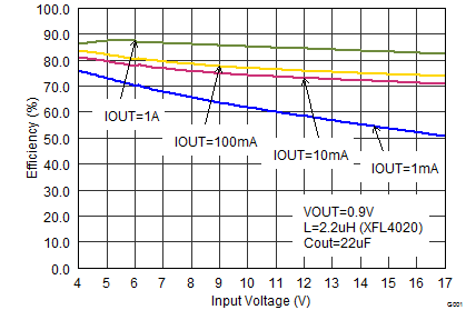
Figure 18. Efficiency With 1.25 MHz, Vout = 0.9 V
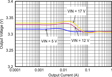
TLV62150 TLV62150A SLVSAL5_loadreg.gif
Figure 20. Output Voltage Accuracy (Load Regulation)
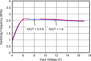
TLV62150 TLV62150A SLVSAL5_fswvin.gif
FSW=Low
Figure 22. Switching Frequency
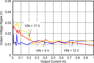
TLV62150 TLV62150A SLVSAL5_voutripple.gif
Figure 24. Output Voltage Ripple
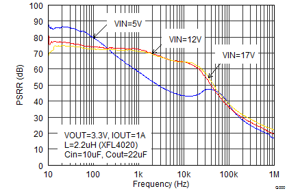
TLV62150 TLV62150A SLVSAL5_psrrhigh.png
IOUT = 1 A
Figure 26. Power Supply Rejection Ratio, FSW = 2.5 MHz
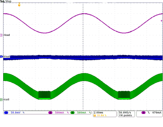
TLV62150 TLV62150A SLVSAL5_mode01.gifFigure 28. PWM-PSM-Transition
(VIN = 12 V, VOUT = 3.3 V With 50 mV/div)
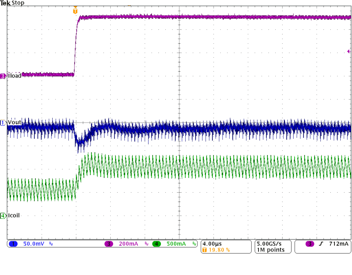
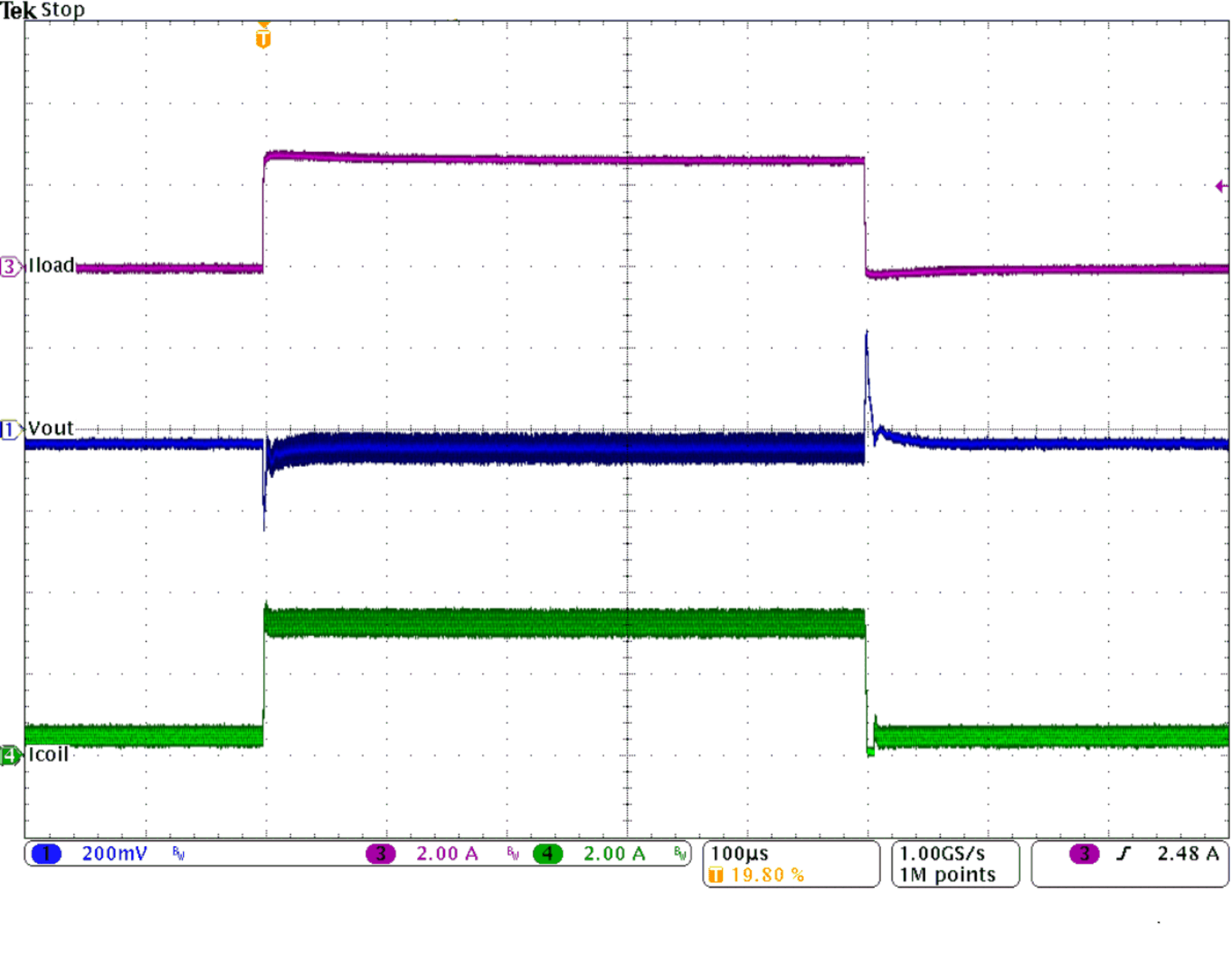
TLV62150 TLV62150A SLVSAL5_loadtranrise.gifFigure 30. Load Transient Response of Figure 29,
Rising Edge
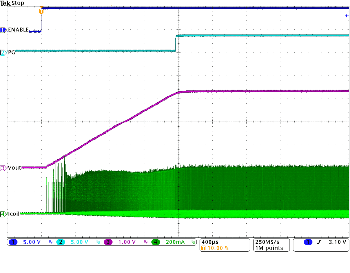
TLV62150 TLV62150A SLVSAL5_stuplow.gifFigure 32. Startup Into 100 mA
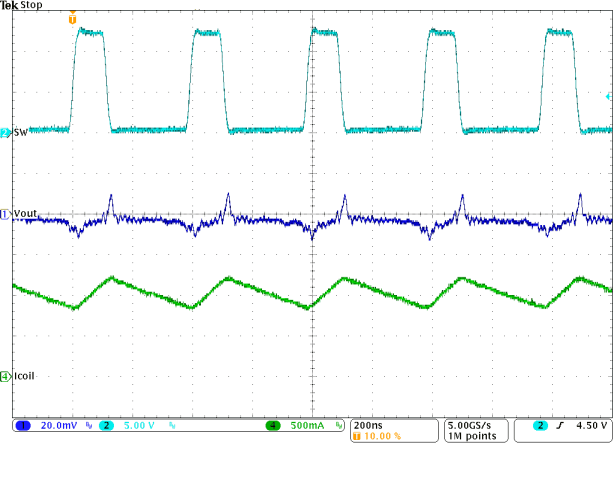
TLV62150 TLV62150A SLVSAL5_PWMtyp.gifFigure 34. Typical Operation In PWM Mode
(IOUT = 1 A)
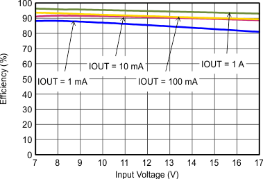
TLV62150 TLV62150A SLVSAL5_eff50vinhalf.gif
Figure 9. Efficiency With 1.25 MHz, Vout = 5 V
TLV62150 TLV62150A SLVSAL5_eff50vinfull.gif
Figure 11. Efficiency With 2.5 MHz, Vout = 5 V
TLV62150 TLV62150A SLVSAL5_eff33vinhalf.gif
Figure 13. Efficiency With 1.25 MHz, Vout = 3.3 V
TLV62150 TLV62150A SLVSAL5_eff33vinfull.gif
Figure 15. Efficiency With 2.5 MHz, Vout = 3.3 V
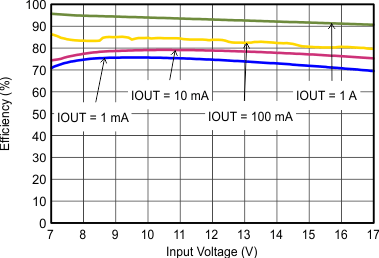
TLV62150 TLV62150A SLVSB71_eff18vinhalf.png
Figure 17. Efficiency With 1.25 MHz, Vout = 1.8 V
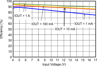
TLV62150 TLV62150A SLVSB71_eff09vinhalf.png
Figure 19. Efficiency With 1.25 MHz, Vout=0.9 V
TLV62150 TLV62150A SLVSAL5_linereg.gif
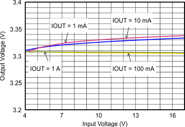
Figure 21. Output Voltage Accuracy (Line Regulation)
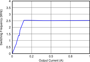
TLV62150 TLV62150A SLVSAL5_fswiout.gif
FSW=Low
Figure 23. Switching Frequency
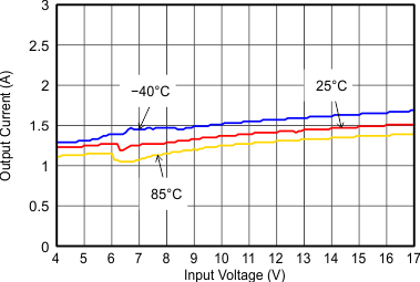
TLV62150 TLV62150A SLVSAL5_ioutmax.gif
Figure 25. Maximum Output Current
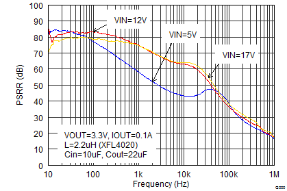
TLV62150 TLV62150A SLVSAL5_psrrlow.png
IOUT = 0.1 A
Figure 27. Power Supply Rejection Ratio, FSW = 2.5 MHz
TLV62150 TLV62150A SLVSAL5_loadtranfull.gifFigure 29. Load Transient Response
(IOUT= 0.5 to 1 to 0.5 A, VIN = 12 V, VOUT = 3.3 V)
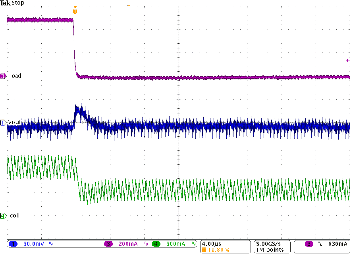
TLV62150 TLV62150A SLVSAL5_loadtranfall.gifFigure 31. Load Transient Response of Figure 29,
Falling Edge
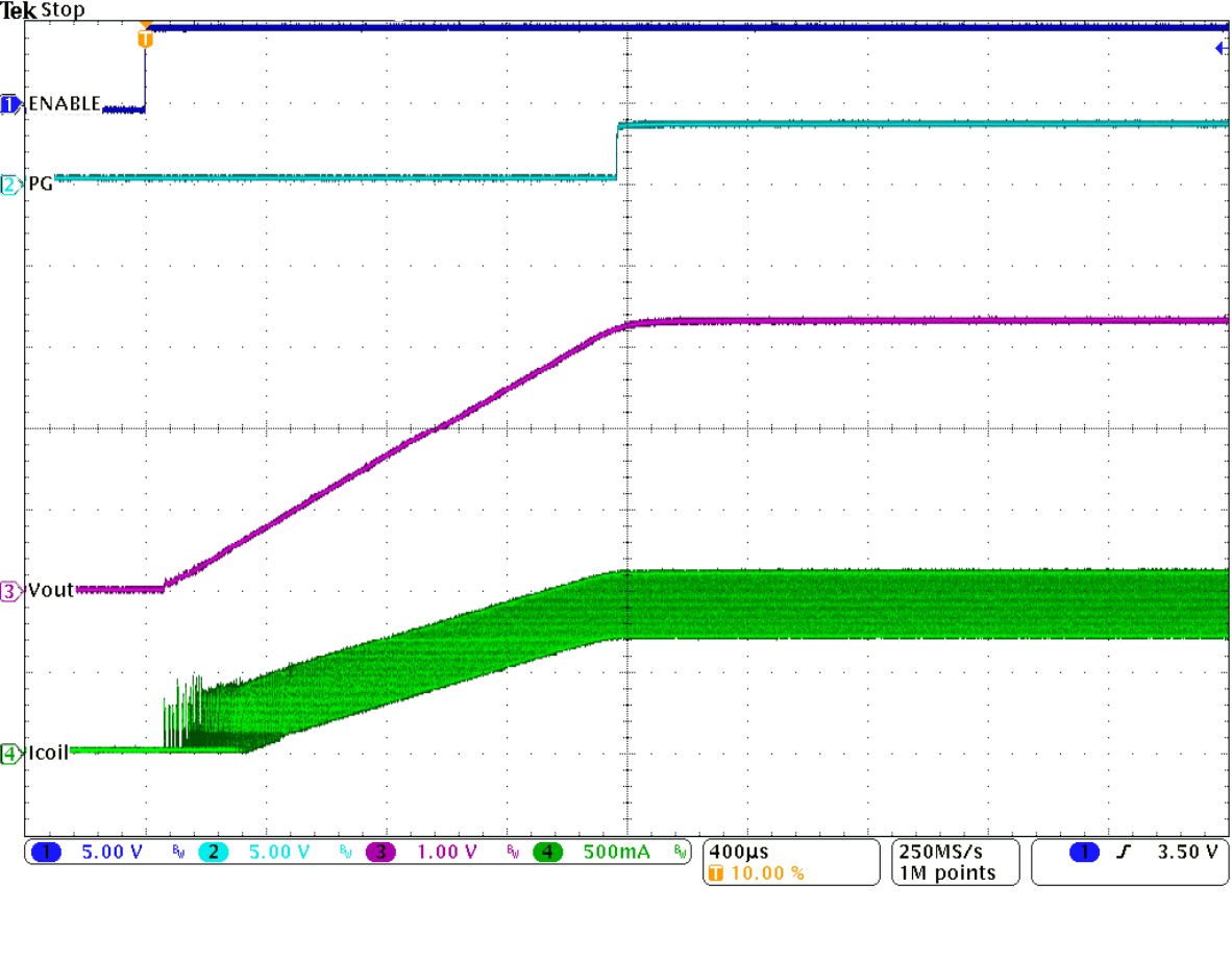
TLV62150 TLV62150A SLVSAL5_stuphigh.gifFigure 33. Startup Into 1 A
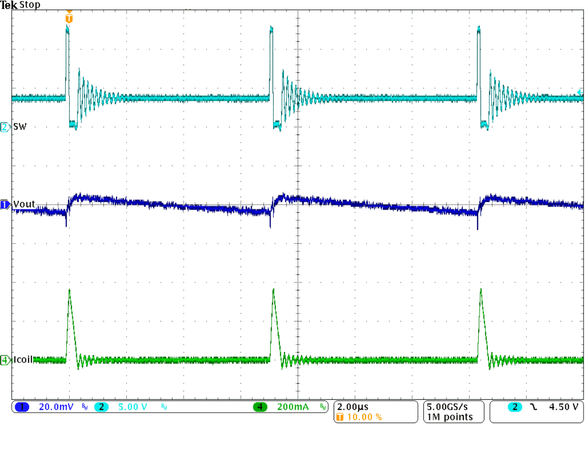
TLV62150 TLV62150A SLVSAL5_PSMtyp.gifFigure 35. Typical Operation in Power Save Mode
(IOUT = 10 mA)