SLVSB76B August   2012  – August 2019 TPS63036

PRODUCTION DATA.  

  1. Features
  2. Applications
  3. Description
    1.     Device Images
      1.      Typical Application Schematic
      2.      Efficiency vs Output Current
  4. Revision History
  5. Pin Configuration and Functions
    1.     Pin Functions
  6. Specifications
    1. 6.1 Absolute Maximum Ratings
    2. 6.2 ESD Ratings
    3. 6.3 Recommended Operating Conditions
    4. 6.4 Thermal Information
    5. 6.5 Electrical Characteristics
    6. 6.6 Typical Characteristics
  7. Detailed Description
    1. 7.1 Overview
    2. 7.2 Functional Block Diagram
    3. 7.3 Feature Description
      1. 7.3.1 Device Enable
      2. 7.3.2 Overvoltage Protection
      3. 7.3.3 Undervoltage Lockout
      4. 7.3.4 Overtemperature Protection
    4. 7.4 Device Functional Modes
      1. 7.4.1 Soft-Start and Short Circuit Protection
      2. 7.4.2 Buck-Boost Operation
      3. 7.4.3 Control Loop
      4. 7.4.4 Power-Save Mode and Synchronization
  8. Application and Implementation
    1. 8.1 Application Information
    2. 8.2 Typical Application
      1. 8.2.1 Design Requirements
      2. 8.2.2 Detailed Design Procedure
        1. 8.2.2.1 Inductor Selection
        2. 8.2.2.2 Capacitor Selection
          1. 8.2.2.2.1 Input Capacitor
          2. 8.2.2.2.2 Output Capacitor
        3. 8.2.2.3 Setting the Output Voltage
        4. 8.2.2.4 Current Limit
      3. 8.2.3 Application Curves
  9. Power Supply Recommendations
  10. 10Layout
    1. 10.1 Layout Guidelines
    2. 10.2 Layout Example
    3. 10.3 Thermal Considerations
  11. 11Device and Documentation Support
    1. 11.1 Device Support
      1. 11.1.1 Third-Party Products Disclaimer
    2. 11.2 Community Resources
    3. 11.3 Trademarks
    4. 11.4 Electrostatic Discharge Caution
    5. 11.5 Glossary
  12. 12Mechanical, Packaging, and Orderable Information

Application Curves

TPS63036 Figure3.gif
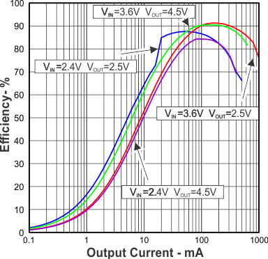
VOUT = 2.5 V/ 4.5 V
Figure 5. Efficiency vs Output Current – Power-Save Mode Enabled
TPS63036 Figure5.gif
VOUT = 3.3 V
Figure 7. Efficiency vs Output Current – Power-Save Mode Enabled
TPS63036 Figure7.gif
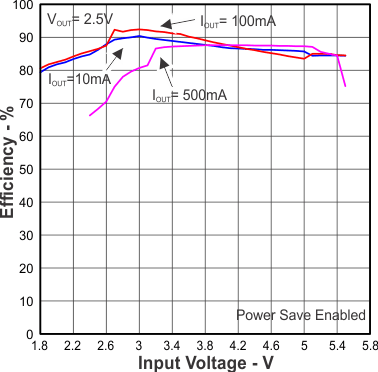
VOUT = 2.5 V, IOUT = 10 mA/100 mA/500 mA
Figure 9. Efficiency vs Input Voltage – Power-Save Mode Enabled
TPS63036 Figure9.gif
VOUT = 3.3 V, IOUT = 10 mA/100 mA/500 mA
Figure 11. Efficiency vs Input Voltage – Power-Save Mode Enabled
TPS63036 Figure11.gif
VOUT = 4.5 V, IOUT = 10 mA/100 mA/500 mA
Figure 13. Efficiency vs Input Voltage – Power-Save Mode Enabled
TPS63036 Figure13.gif
VOUT = 2.5 V
Figure 15. Output Voltage vs Output Current
TPS63036 Figure15.gif
VOUT = 4.5 V
Figure 17. Output Voltage vs Output Current
TPS63036 Figure151.gif
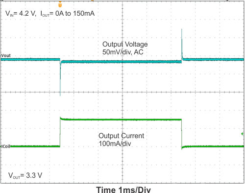
VIN > VOUT, Load Change from 0 mA to 150 mA
Figure 19. Load Transient Response
TPS63036 Figure19.gif
VOUT = 3.3 V, VIN = 2.4 V, RL = 33 Ω
Figure 21. Start-Up After Enable
TPS63036 Figure4.gif
VOUT = 2.5 V/ 4.5 V
Figure 6. Efficiency vs Output Current – Power-Save Mode Disabled
TPS63036 Figure6.gif
VOUT = 3.3 V
Figure 8. Efficiency vs Output Current – Power-Save Mode Disabled
TPS63036 Figure8.gif
VOUT = 2.5 V, IOUT = 10 mA/100 mA/500 mA
Figure 10. Efficiency vs Input Voltage – Power-Save Mode Disabled
TPS63036 Figure10.gif
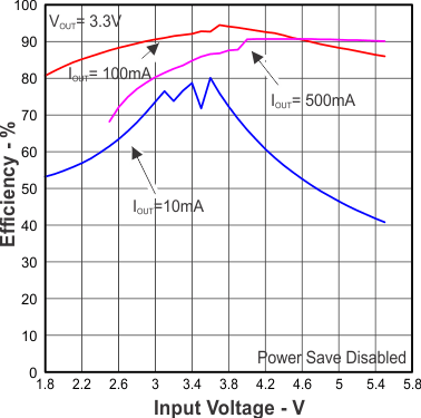
VOUT = 3.3 V, IOUT = 10 mA/100 mA/500 mA
Figure 12. Efficiency vs Input Voltage – Power-Save Mode Disabled
TPS63036 Figure12.gif
VOUT = 4.5 V, IOUT = 10 mA/100 mA/500 mA
Figure 14. Efficiency vs Input Voltage – Power-Save Mode Disabled
TPS63036 Figure14.gif
VOUT = 3.3 V
Figure 16. Output Voltage vs Output Current
TPS63036 Figure161.gif
VIN < VOUT, Load Change from 0 mA to 150 mA
Figure 18. Load Transient Response
TPS63036 Figure181.gif
VOUT = 3.3 V, IOUT = 150 mA
Figure 20. Line Transient Response
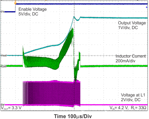
TPS63036 Figure20.gif
VOUT = 3.3 V, VIN = 4.2 V, RL = 33 Ω
Figure 22. Start-Up After Enable