SLVSBO7O December   2012  – August 2024 TPD1E05U06 , TPD4E05U06 , TPD6E05U06

PRODUCTION DATA  

  1.   1
  2. Features
  3. Applications
  4. Description
  5. Pin Configuration and Functions
  6. Specifications
    1.     Absolute Maximum Ratings
    2. 5.1 ESD Ratings—JEDEC Specification
    3. 5.2 ESD Ratings—IEC Specification
    4.     Recommended Operating Conditions
    5. 5.3 Thermal Information
    6. 5.4 Electrical Characteristics
    7. 5.5 Typical Characteristics
  7. Detailed Description
    1. 6.1 Overview
    2. 6.2 Functional Block Diagram
    3. 6.3 Feature Description
      1. 6.3.1 ±15-kV IEC61000-4-2 Level 4 ESD Protection
      2. 6.3.2 IEC61000-4-4 EFT Protection
      3. 6.3.3 IEC61000-4-5 Surge Protection
      4. 6.3.4 I/O Capacitance
      5. 6.3.5 DC Breakdown Voltage
      6. 6.3.6 Ultra-Low Leakage Current
      7. 6.3.7 Low ESD Clamping Voltage
      8. 6.3.8 Industrial Temperature Range
      9. 6.3.9 Easy Flow-Through Routing
    4. 6.4 Device Functional Modes
  8. Application and Implementation
    1. 7.1 Application Information
    2. 7.2 Typical Applications
      1. 7.2.1 HDMI 2.0 Application
        1. 7.2.1.1 Design Requirements
        2. 7.2.1.2 Detailed Design Procedure
          1. 7.2.1.2.1 Signal Range on Pin 1, 2, 4, or 5
        3. 7.2.1.3 Application Curves
      2. 7.2.2 HDMI 2.0 Application
        1. 7.2.2.1 Design Requirements
        2. 7.2.2.2 Detailed Design Procedure
          1. 7.2.2.2.1 Signal Range
          2. 7.2.2.2.2 Operating Frequency
        3. 7.2.2.3 Application Curves
    3. 7.3 Power Supply Recommendations
    4. 7.4 Layout
      1. 7.4.1 Layout Guidelines
      2. 7.4.2 Layout Example
        1. 7.4.2.1 TPD4E05U06 Layout Example
        2. 7.4.2.2 TPD1E05U06 Layout Example
  9. Device and Documentation Support
    1. 8.1 Documentation Support
      1. 8.1.1 Related Documentation
    2. 8.2 Receiving Notification of Documentation Updates
    3. 8.3 Support Resources
    4. 8.4 Trademarks
    5. 8.5 Electrostatic Discharge Caution
    6. 8.6 Glossary
  10. Revision History
  11. 10Mechanical, Packaging, and Orderable Information
    1. 10.1 Tape and Reel Information
    2. 10.2 Mechanical Data

Typical Characteristics

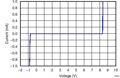
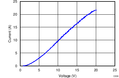
TPD1E05U06 TPD4E05U06 TPD6E05U06 DC Voltage Sweep I-V CurveFigure 5-1 DC Voltage Sweep I-V Curve
TPD1E05U06 TPD4E05U06 TPD6E05U06 Positive TLP Plot IO to GNDFigure 5-3 Positive TLP Plot IO to GND
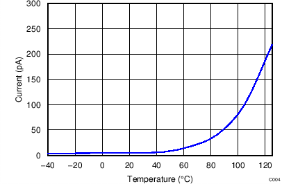
TPD1E05U06 TPD4E05U06 TPD6E05U06 Leakage vs TemperatureFigure 5-5 Leakage vs Temperature
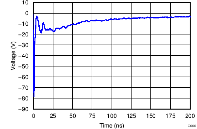
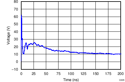
TPD1E05U06 TPD4E05U06 TPD6E05U06 –8-kV IEC WaveformFigure 5-7 –8-kV IEC Waveform
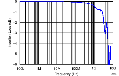
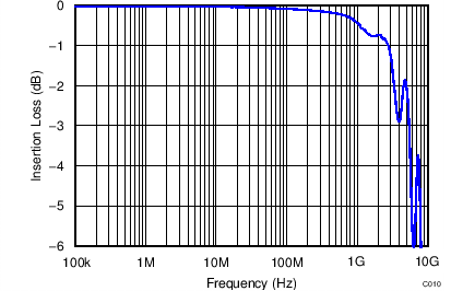
TPD1E05U06 TPD4E05U06 TPD6E05U06 TPD4E05U06 Insertion LossFigure 5-9 TPD4E05U06 Insertion Loss
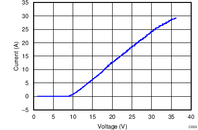
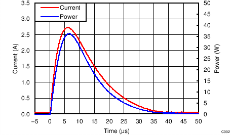
TPD1E05U06 TPD4E05U06 TPD6E05U06 Surge Curve (tp = 8/20 μs), Pin IO to GNDFigure 5-2 Surge Curve (tp = 8/20 μs), Pin IO to GND
TPD1E05U06 TPD4E05U06 TPD6E05U06 Negative TLP Plot IO to GNDFigure 5-4 Negative TLP Plot IO to GND
TPD1E05U06 TPD4E05U06 TPD6E05U06 8-kV IEC WaveformFigure 5-6 8-kV IEC Waveform
TPD1E05U06 TPD4E05U06 TPD6E05U06 TPD1E05U06 Insertion LossFigure 5-8 TPD1E05U06 Insertion Loss
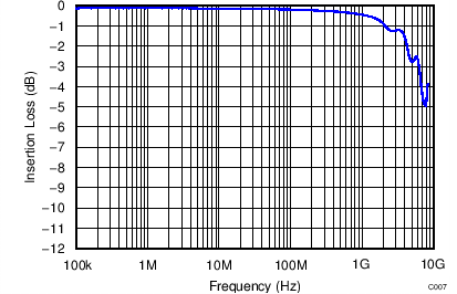
TPD1E05U06 TPD4E05U06 TPD6E05U06 TPD6E05U06 Insertion LossFigure 5-10 TPD6E05U06 Insertion Loss