SLVSC26B November 2013 – May 2024 TPS61162A , TPS61163A
PRODUCTION DATA
- 1
- 1 Features
- 2 Applications
- 3 Description
- 4 Pin Configuration and Functions
- 5 Specifications
- 6 Detailed Description
- 7 Application and Implementation
- 8 Device and Documentation Support
- 9 Revision History
- 10Mechanical, Packaging, and Orderable Information
7.2.4 Additional Application Circuits
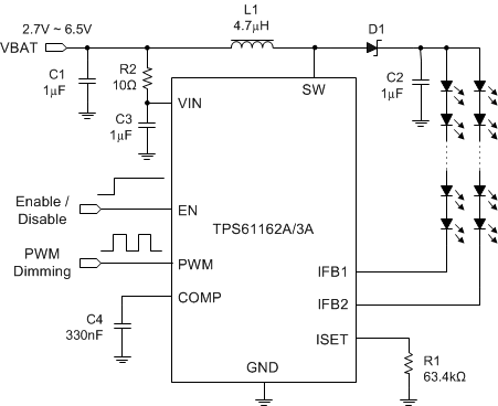
In Figure 7-13 the PWM Interface is enabled, and the PWM input signal is used to adjust the brightness level. The PWM pin as well as the EN pin can be used to enable or disable the TPS61162A, TPS61163A.
 Figure 7-13 TPS61162A/TPS61163A Typical Application
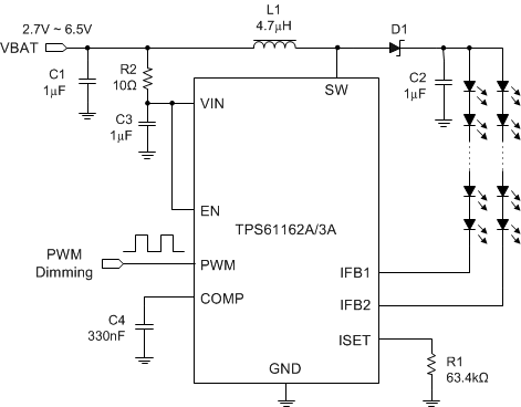
Figure 7-14 shows PWM interface enabled, EN pin connected to VIN, with only the PWM Signal used to adjust the brightness level and to enable or disable the TPS61162A, TPS61163A.
 Figure 7-14 TPS61162A/TPS61163A Typical Application
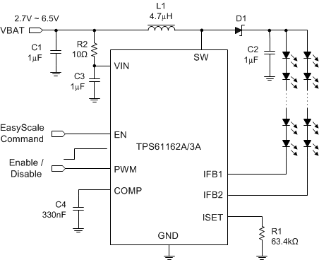
In Figure 7-15 the one-wire digital interface is enabled. Brightness level is adjusted with the PWM pin using EasyScale commands. The PWM signal must remain high for the device to be enabled.
 Figure 7-15 TPS61162A/TPS61163A Typical Application
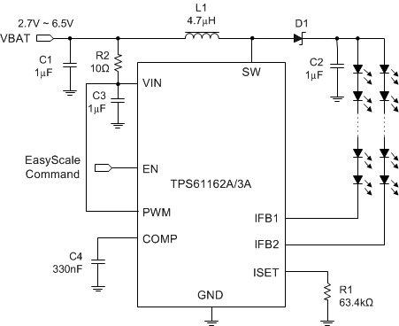
Figure 7-16 shows one-wire digital interface enabled, PWM pin connected to VIN, with only the EN signal used to enable or disable the device. Brightness level adjustments (using EasyScale Commands) can be achieved via the EN pin only.
 Figure 7-16 TPS61162A/TPS61163A Typical Application