SLVSC26B November 2013 – May 2024 TPS61162A , TPS61163A
PRODUCTION DATA
- 1
- 1 Features
- 2 Applications
- 3 Description
- 4 Pin Configuration and Functions
- 5 Specifications
- 6 Detailed Description
- 7 Application and Implementation
- 8 Device and Documentation Support
- 9 Revision History
- 10Mechanical, Packaging, and Orderable Information
6.3.8 Overvoltage Protection
Overvoltage protection circuitry prevents device damage as the result of white LED string disconnection or shortage.
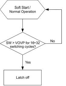
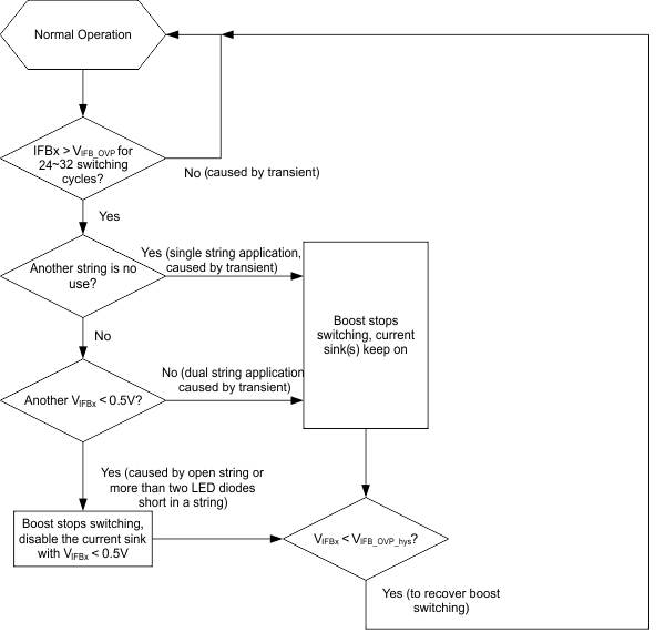
The TPS61162A/TPS61163A monitors the voltages at SW pin and IFBx pin during each switching cycle. No matter either SW OVP threshold VOVP_SW or IFBx OVP threshold VOVP_FB is reached due to the LED string open or short issue, the protection circuitry will be triggered. Refer to Figure 6-1 and Figure 6-2 for the protection actions.
If one LED string is open, its IFBx pin voltage drops, and the boost output voltage is increased by the control loop as it tries to regulate this lower IFBx voltage to the target value (90mV typical). For the normal string, its current is still under regulation but its IFBx voltage increases along with the output voltage. During the process, either the SW voltage reaches its OVP threshold VOVP_SW or the normal string’s IFBx pin voltage reaches the IFBx OVP threshold VOVP_FB, then the protection circuitry will be triggered accordingly.
If both LED strings are open, both IFBx pins’ voltages drop to ground, and the boost output voltage is increased by the control loop until reaching the SW OVP threshold VOVP_SW, the SW OVP protection circuitry is triggered, and the device is latched off. Only VIN POR or EN/PWM pin toggling can restart the IC.
One LED diode short in a string is allowed for the TPS61162A, TPS61163A. If one LED diode in a string is short, the normal string’s IFBx voltage is regulated to about 90 mV, and the abnormal string’s IFBx pin voltage will be higher. Normally with only one diode short, the higher IFBx pin voltage does not reach the IFBx OVP threshold VOVP_FB, so the protection circuitry will not be triggered.
If more than one LED diodes are short in a string, as the boost loop regulates the normal string’s IFBx voltage to 90 mV, this abnormal string’s IFBx pin voltage is much higher and will reach VOVP_FB, then the protection circuitry is triggered.
The SW OVP protection will also be triggered when the forward voltage drop of an LED string exceeds the SW OVP threshold. In this case, the device turns off the switch FET and shuts down.
 Figure 6-1 SW OVP Action
 Figure 6-2 VIFBx OVP Action