SLVSC26B November 2013 – May 2024 TPS61162A , TPS61163A
PRODUCTION DATA
- 1
- 1 Features
- 2 Applications
- 3 Description
- 4 Pin Configuration and Functions
- 5 Specifications
- 6 Detailed Description
- 7 Application and Implementation
- 8 Device and Documentation Support
- 9 Revision History
- 10Mechanical, Packaging, and Orderable Information
6.5.1 EasyScale Programming
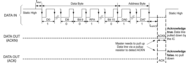
EasyScale is a simple, but flexible, one-pin interface to configure the current of the dual channels. The interface is based on a master-slave structure, where the master is typically a microcontroller or application processor and the device is the slave. Figure 6-5 and Table 6-1 give an overview of the protocol used by TPS61162A/TPS61163A. A command consists of 24 bits, including an 8-bit device address byte and a 16-bit data byte. All of the 24 bits should be transmitted together each time, and the LSB bit should be transmitted first. The device address byte D7(MSB)~D0(LSB) is fixed to 0x8F. The data byte includes 9 bits D8(MSB)~D0(LSB) for brightness information and an RFA bit. The RFA bit set to "1" indicates the Request for Acknowledge condition. The Acknowledge condition is only applied when the protocol is received correctly. The advantage of EasyScale compared with other one pin interfaces is that its bit detection is in a large extent independent from the bit transmission rate. It can automatically detect bit rates between 1.7kBit/sec and up to 160kBit/sec.
 Figure 6-5 Easyscale Protocol Overview
| BYTE | BIT NUMBER | NAME | TRANSMISSION DIRECTION | DESCRIPTION |
|---|---|---|---|---|
| Device Address Byte (0x8F) | 23 (MSB) | DA7 | IN | DA7 = 1, MSB of device address |
| 22 | DA6 | DA6 = 0 | ||
| 21 | DA5 | DA5 = 0 | ||
| 20 | DA4 | DA4 = 0 | ||
| 19 | DA3 | DA3 = 1 | ||
| 18 | DA2 | DA2 = 1 | ||
| 17 | DA1 | DA1 = 1 | ||
| 16 | DA0 | DA0 = 1, LSB of device address | ||
| Data Byte | 15 | Bit 15 | IN | No information. Write 0 to this bit. |
| 14 | Bit 14 | No information. Write 0 to this bit. | ||
| 13 | Bit 13 | No information. Write 0 to this bit. | ||
| 12 | Bit 12 | No information. Write 0 to this bit. | ||
| 11 | Bit 11 | No information. Write 0 to this bit. | ||
| 10 | RFA | Request for acknowledge. If set to 1, device will pull low the data line when it receives the command well. This feature can only be used when the master has an open drain output stage and the data line needs to be pulled high by the master with a pullup resistor; otherwise, acknowledge condition is not allowed and don't set this bit to 1. | ||
| 9 | Bit 9 | No information. Write 0 to this bit. | ||
| 8 | D8 | Data bit 8, MSB of brightness code | ||
| 7 | D7 | Data bit 7 | ||
| 6 | D6 | Data bit 6 | ||
| 5 | D5 | Data bit 5 | ||
| 4 | D4 | Data bit 4 | ||
| 3 | D3 | Data bit 3 | ||
| 2 | D2 | Data bit 2 | ||
| 1 | D1 | Data bit 1 | ||
| 0 (LSB) | D0 | Data bit 0, LSB of brightness code |
 Figure 6-6 Easyscale Timing, With RFA = 0
 Figure 6-7 Easyscale Timing, With RFA = 1
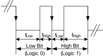
 Figure 6-8 Easyscale — Bit Coding
The 24-bit command should be transmitted with LSB first and MSB last. Figure 6-6 shows the protocol without acknowledge request (Bit RFA = 0), Figure 6-7 with acknowledge request (Bit RFA = 1). Before the command transmission, a start condition must be applied. For this, the EN pin must be pulled high for at least tstart (2μs) before the bit transmission starts with the falling edge. If the EN pin is already at high level, no start condition is needed. The transmission of each command is closed with an End of Stream condition for at least tEOS (2μs).
The bit detection is based on a Logic Detection scheme, where the criterion is the relation between tLOW and tHIGH (refer to Figure 6-8). It can be simplified to:
Low Bit (Logic 0): tLOW ≥ 2 x tHIGH
High Bit (Logic 1): tHIGH ≥ 2 x tLOW
The bit detection starts with a falling edge on the EN pin and ends with the next falling edge. Depending on the relation between tHIGH and tLOW, the logic 0 or 1 is detected.
The acknowledge condition is only applied if:
- Acknowledge is requested by setting RFA bit to 1.
- The transmitted device address matches with the device address of the IC.
- Total 24 bits are received correctly.
If above conditions are met, after tvalACK delay from the moment when the last falling edge of the protocol is detected, an internal ACKN-MOSFET is turned on to pull the EN pin low for the time tACKN, which is 512μs maximum, then the Acknowledge condition is valid. During the tvalACK delay, the master controller keeps the line low; after the delay, it should release the line by outputting high impedance and then detect the acknowledge condition. If it reads back a logic 0, it means the device has received the command correctly. The EN pin can be used again by the master when the acknowledge condition ends after tACKN time.
The acknowledge condition can only be requested when the master device has an open drain output. For a push-pull output stage, the use of a series resistor in the EN line to limit the current to 500μA is recommended to for such cases as:
- An accidentally requested acknowledge, or
- To protect the internal ACKN-MOSFET.