SLVSCE8C January 2015 – September 2018 TPS7B7701-Q1 , TPS7B7702-Q1
PRODUCTION DATA.
- 1 Features
- 2 Applications
- 3 Description
- 4 Revision History
- 5 Pin Configuration and Functions
- 6 Specifications
-
7 Detailed Description
- 7.1 Overview
- 7.2 Functional Block Diagram
- 7.3
Feature Description
- 7.3.1 Fault Detection and Protection
- 7.3.2 Short-Circuit and Overcurrent Protection
- 7.3.3 Short-to-Battery and Reverse Current Detection
- 7.3.4 Thermal Shutdown
- 7.3.5 Integrated Reverse-Polarity Protection
- 7.3.6 Integrated Inductive Clamp
- 7.3.7 Undervoltage Lockout
- 7.3.8 Enable (EN, EN1, and EN2)
- 7.3.9 Internal Voltage Regulator (VCC)
- 7.3.10 Current Sense Multiplexing
- 7.3.11 Adjustable Output Voltage (FB, FB1, and FB2)
- 7.4 Device Functional Modes
- 8 Application and Implementation
- 9 Power Supply Recommendations
- 10Layout
- 11Device and Documentation Support
- 12Mechanical, Packaging, and Orderable Information
7.3.10 Current Sense Multiplexing
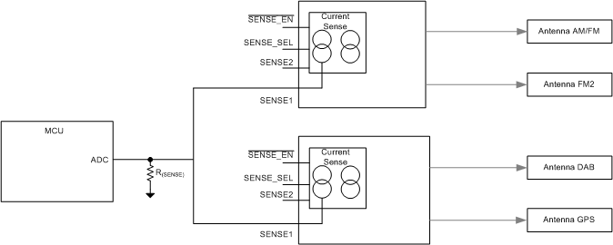
The two, independent current sense pins (one for each channel) provide flexibility in the system design. When the ADC resource is limited, the device allows the multiplexing of the current sense pins by only using one current sense pin and one ADC to monitor all the antenna outputs.
The SENSE_SEL pin (TPS7B7702-Q1 only) selects the channels to monitor the current. The SENSE_EN pin enables and disables the SENSE pin, allowing multiplexing between chips. Therefore, only one ADC and one resistor is needed for current-sense diagnostics of multiple outputs. When the SENSE1 pin is connected to an ADC, the current flow through both channels can be sensed by changing the electrical level at the SENSE_SEL pin.
Table 2 lists the selection logic for the current sense.
Table 2. SENSE_EN and SEN_SEL Logic Table
| SENSE_EN | SEN_SEL | SENSE1 Status | SENSE2 Status |
|---|---|---|---|
| LOW | LOW | CH1 current | CH2 current |
| LOW | HIGH | CH2 current | HIGH impedance |
| HIGH | — | HIGH impedance | HIGH impedance |
Figure 20 shows the application of four antenna channels sharing one ADC resource.
 Figure 20. Current Multiplexing Application Block