SLVSD05G March 2016 – August 2024 TPS56C215
PRODUCTION DATA
- 1
- 1 Features
- 2 Applications
- 3 Description
- 4 Pin Configuration and Functions
- 5 Specifications
-
6 Detailed Description
- 6.1 Overview
- 6.2 Functional Block Diagram
- 6.3
Feature Description
- 6.3.1 PWM Operation and D-CAP3™ Control Mode
- 6.3.2 Eco-mode Control
- 6.3.3 4.7-V LDO
- 6.3.4 MODE Selection
- 6.3.5 Soft Start and Prebiased Soft Start
- 6.3.6 Enable and Adjustable UVLO
- 6.3.7 Power Good
- 6.3.8 Overcurrent Protection and Undervoltage Protection
- 6.3.9 UVLO Protection
- 6.3.10 Thermal Shutdown
- 6.3.11 Output Voltage Discharge
- 6.4 Device Functional Modes
- 7 Application and Implementation
- 8 Device and Documentation Support
- 9 Revision History
- 10Mechanical, Packaging, and Orderable Information
3 Description
The TPS56C215 is a small monolithic 12A synchronous buck converter with an adaptive on-time D-CAP3 control mode. The device integrates low RDS(on) power MOSFETs that enable high efficiency and offers ease-of-use with minimum external component count for space-conscious power systems. Competitive features include a very accurate reference voltage, fast load transient response, auto-skip mode operation for light load efficiency, adjustable current limit and no requirement for external compensation. A forced continuous conduction mode helps meet tight voltage regulation accuracy requirements for performance DSPs and FPGAs. The TPS56C215 is available in a thermally enhanced, 18-pin, HotRod QFN package and is designed to operate from –40°C to 150°C junction temperature.
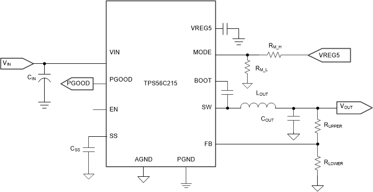
 Typical Application
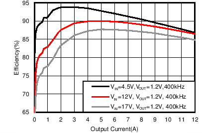
 Efficiency vs Output Current