SLVSDC7G April   2017  – July 2024 DRV5032

PRODUCTION DATA  

  1.   1
  2. Features
  3. Applications
  4. Description
  5. Device Comparison
  6. Pin Configuration and Functions
  7. Specifications
    1. 6.1 Absolute Maximum Ratings
    2. 6.2 ESD Ratings
    3. 6.3 Recommended Operating Conditions
    4. 6.4 Thermal Information
    5. 6.5 Electrical Characteristics
    6. 6.6 Magnetic Characteristics
    7. 6.7 Typical Characteristics
  8. Detailed Description
    1. 7.1 Overview
    2. 7.2 Functional Block Diagram
    3. 7.3 Feature Description
      1. 7.3.1 Magnetic Flux Direction
      2. 7.3.2 Device Version Comparison
        1. 7.3.2.1 Magnetic Threshold
        2. 7.3.2.2 Magnetic Response
        3. 7.3.2.3 Output Type
        4. 7.3.2.4 Sampling Rate
      3. 7.3.3 Hall Element Location
    4. 7.4 Device Functional Modes
  9. Application and Implementation
    1. 8.1 Application Information
      1. 8.1.1 Output Type Tradeoffs
    2. 8.2 Typical Applications
      1. 8.2.1 General-Purpose Magnet Sensing
        1. 8.2.1.1 Design Requirements
        2. 8.2.1.2 Detailed Design Procedure
        3. 8.2.1.3 Application Curve
      2. 8.2.2 Three-Position Switch
        1. 8.2.2.1 Design Requirements
        2. 8.2.2.2 Detailed Design Procedure
        3. 8.2.2.3 Application Curve
    3. 8.3 Best Design Practices
    4. 8.4 Power Supply Recommendations
    5. 8.5 Layout
      1. 8.5.1 Layout Guidelines
      2. 8.5.2 Layout Examples
  10. Device and Documentation Support
    1. 9.1 Documentation Support
      1. 9.1.1 Related Documentation
    2. 9.2 Receiving Notification of Documentation Updates
    3. 9.3 Support Resources
    4. 9.4 Trademarks
    5. 9.5 Electrostatic Discharge Caution
    6. 9.6 Glossary
  11. 10Revision History
  12. 11Mechanical, Packaging, and Orderable Information

Description

The DRV5032 device is an ultra-low-power digital-switch Hall effect sensor, designed for the most compact and battery-sensitive systems. The device is offered in multiple magnetic thresholds, sampling rates, output drivers, and packages to accommodate various applications.

When the applied magnetic flux density exceeds the BOP threshold, the device outputs a low voltage. The output stays low until the flux density decreases to less than BRP, and then the output either drives a high voltage or becomes high impedance, depending on the device version. By incorporating an internal oscillator, the device samples the magnetic field and updates the output at a rate of 80Hz, 20Hz or 5Hz for the lowest current consumption. Omnipolar and unipolar magnetic responses are available.

The device operates from a VCC range of 1.65V to 5.5V, and is packaged in a standard SOT-23, TO-92 and small X2SON.

Package Information
PART NUMBER PACKAGE(1) PACKAGE SIZE(2)
DRV5032 DBZ (SOT-23, 3) 2.92mm × 2.37mm
DMR (X2SON, 4) 1.4mm × 1.1mm
LPG (TO-92, 3) 4mm × 1.52mm
For all available packages, see the orderable addendum at the end of the data sheet.
The package size (length × width) is a nominal value and includes pins, where applicable.
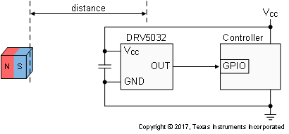
DRV5032  Typical Schematic Typical Schematic
DRV5032  Current Consumption of 5Hz Version Current Consumption of 5Hz Version