SLVSDD0B May 2016 – September 2017 TPS22975
PRODUCTION DATA.
- 1 Features
- 2 Applications
- 3 Description
- 4 Revision History
- 5 Device Comparison Table
- 6 Pin Configuration and Functions
- 7 Specifications
- 8 Parameter Measurement Information
- 9 Detailed Description
- 10Application and Implementation
- 11Power Supply Recommendations
- 12Layout
- 13Device and Documentation Support
- 14Mechanical, Packaging, and Orderable Information
9 Detailed Description
9.1 Overview
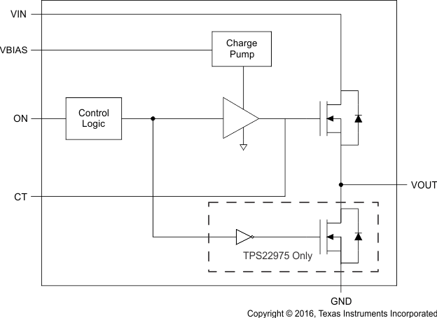
The TPS22975 device is a single-channel, 6-A load switch in an 8-pin SON package. To reduce the voltage drop in high current rails, the device implements an N-channel MOSFET. The device has a configurable slew rate for applications that require a specific rise-time.
The device prevents downstream circuits from pulling high standby current from the supply by limiting the leakage current of the device when it is disabled. The integrated control logic, driver, power supply, and output discharge FET eliminates the need for any external components, which reduces solution size and bill of materials (BOM) count.
9.2 Functional Block Diagram

9.3 Feature Description
9.3.1 Adjustable Rise Time
A capacitor to GND on the CT pin sets the slew rate. The voltage on the CT pin can be as high as 15 V; therefore, the minimum voltage rating for the CT capacitor must be 30 V for optimal performance. An approximate formula for the relationship between CT and slew rate when VBIAS is set to 5 V is shown in Equation 1. This equation accounts for 10% to 90% measurement on VOUT and does not apply for CT < 100 pF. Use Table 1 to determine rise times for when CT = 0 pF.

where
- SR is the slew rate (in µs/V)
- CT is the capacitance value on the CT pin (in pF)
- The units for the constant 26 are µs/V. The units for the constant 0.43 are µs/(V × pF).
Rise time can be calculated by multiplying the input voltage by the slew rate. Table 1 contains rise time values measured on a typical device. Rise times shown in Table 1 are only valid for the power-up sequence where VIN and VBIAS are already in steady state condition before the ON pin is asserted high.
Table 1. Rise Time tR vs CT Capacitor
| CT (pF) | RISE TIME (µs) 10% - 90%, CL = 0.1 µF, CIN = 1 µF, RL = 10 Ω, VBIAS = 5 V(1) | ||||||
|---|---|---|---|---|---|---|---|
| VIN = 5 V | VIN = 3.3 V | VIN = 1.8 V | VIN = 1.5 V | VIN = 1.2 V | VIN = 1.05 V | VIN = 0.6 V | |
| 0 | 140 | 105 | 75 | 65 | 60 | 55 | 40 |
| 220 | 520 | 360 | 215 | 185 | 160 | 140 | 95 |
| 470 | 970 | 660 | 385 | 330 | 275 | 240 | 155 |
| 1000 | 1750 | 1190 | 700 | 595 | 495 | 435 | 275 |
| 2200 | 3875 | 2615 | 1520 | 1290 | 1070 | 940 | 595 |
| 4700 | 7580 | 5110 | 2950 | 2510 | 2075 | 1830 | 1150 |
| 10000 | 16980 | 11485 | 6650 | 5635 | 4685 | 4110 | 2595 |
9.3.2 Quick-Output Discharge (QOD) (Optional)
The TPS22975 includes an optional QOD feature. When the switch is disabled, an internal discharge resistance is connected between VOUT and GND to remove the remaining charge from the output. This resistance has a typical value of 230 Ω and prevents the output from floating while the switch is disabled. For best results, it is recommended that the device gets disabled before VBIAS falls below the minimum recommended voltage.
9.3.3 Thermal Shutdown
Thermal shutdown protects the part from internally or externally generated excessive temperatures. When the device temperature triggers TSD (typical 160°C), the switch is turned off. The switch automatically turns on again if the temperature of the die drops 20 degrees below the TSD threshold.
9.4 Device Functional Modes
The Table 2 lists the VOUT pin states as determined by the ON pin.
Table 2. VOUT Connection
| ON | TPS22975 | TPS22975N |
|---|---|---|
| L | GND | Open |
| H | VIN | VIN |