SLVSDD1G December   2017  – June 2024 TPS62800 , TPS62801 , TPS62802 , TPS62806 , TPS62807 , TPS62808

PRODUCTION DATA  

  1.   1
  2. Features
  3. Applications
  4. Description
  5. Device Comparison Table
  6. Pin Configuration and Functions
  7. Specifications
    1. 6.1 Absolute Maximum Ratings
    2. 6.2 ESD Ratings
    3. 6.3 Recommended Operating Conditions
    4. 6.4 Thermal Information
    5. 6.5 Electrical Characteristics
    6. 6.6 Typical Characteristics
  8. Detailed Description
    1. 7.1 Overview
    2. 7.2 Functional Block Diagram
    3. 7.3 Feature Description
      1. 7.3.1 Smart Enable and Shutdown (EN)
      2. 7.3.2 Soft Start
      3. 7.3.3 VSEL/MODE Pin
        1. 7.3.3.1 Output Voltage Selection (R2D Converter)
        2. 7.3.3.2 Mode Selection — Power Save Mode and Forced PWM Operation
      4. 7.3.4 Undervoltage Lockout (UVLO)
      5. 7.3.5 Switch Current Limit and Short Circuit Protection
      6. 7.3.6 Thermal Shutdown
      7. 7.3.7 Output Voltage Discharge
    4. 7.4 Device Functional Modes
      1. 7.4.1 Power Save Mode Operation
      2. 7.4.2 Forced PWM Mode Operation
      3. 7.4.3 100% Mode Operation
      4. 7.4.4 Optimized Transient Performance from PWM-to-PFM Mode Operation
  9. Application and Implementation
    1. 8.1 Application Information
    2. 8.2 Typical Application
      1. 8.2.1 Design Requirements
      2. 8.2.2 Detailed Design Procedure
        1. 8.2.2.1 Custom Design With WEBENCH® Tools
        2. 8.2.2.2 Inductor Selection
        3. 8.2.2.3 Output Capacitor Selection
        4. 8.2.2.4 Input Capacitor Selection
      3. 8.2.3 Application Curves
    3. 8.3 System Examples
    4. 8.4 Power Supply Recommendations
    5. 8.5 Layout
      1. 8.5.1 Layout Guidelines
      2. 8.5.2 Layout Example
  10. Device and Documentation Support
    1. 9.1 Device Support
      1. 9.1.1 Third-Party Products Disclaimer
      2. 9.1.2 Development Support
        1. 9.1.2.1 Custom Design With WEBENCH® Tools
    2. 9.2 Receiving Notification of Documentation Updates
    3. 9.3 Support Resources
    4. 9.4 Trademarks
    5. 9.5 Electrostatic Discharge Caution
    6. 9.6 Glossary
  11. 10Revision History
  12. 11Mechanical, Packaging, and Orderable Information
    1. 11.1 Mechanical Data

Typical Characteristics

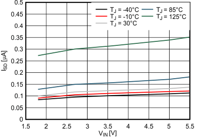
TPS62800 TPS62801 TPS62802 TPS62806 TPS62807 TPS62808 Shutdown Current,
                            ISD
EN = GND
Figure 6-1 Shutdown Current, ISD
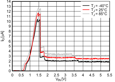
TPS62800 TPS62801 TPS62802 TPS62806 TPS62807 TPS62808 Operating Quiescent
                        Current, IQ
VIN fallingDevice switching, no load, VOUT = 1.2 V
EN = VINVSEL/MODE = GND
Figure 6-3 Operating Quiescent Current, IQ
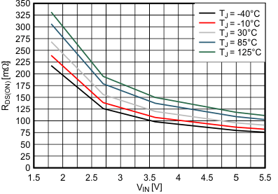
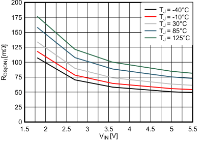
TPS62800 TPS62801 TPS62802 TPS62806 TPS62807 TPS62808 High-Side Switch Drain
                        Source Resistance, RDS(ON)
Figure 6-5 High-Side Switch Drain Source Resistance, RDS(ON)
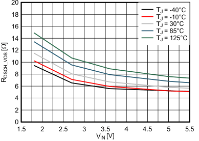
TPS62800 TPS62801 TPS62802 TPS62806 TPS62807 TPS62808 VOS Discharge Switch
                        Drain Source Resistance, RDSCH_VOS
Figure 6-7 VOS Discharge Switch Drain Source Resistance, RDSCH_VOS
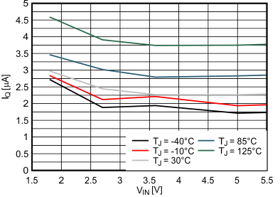
TPS62800 TPS62801 TPS62802 TPS62806 TPS62807 TPS62808 Quiescent Current,
                            IQ
Device not switching
Figure 6-2 Quiescent Current, IQ
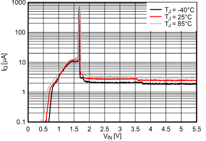
TPS62800 TPS62801 TPS62802 TPS62806 TPS62807 TPS62808 Operating Quiescent
                        Current, IQ
VIN risingDevice switching, no load, VOUT = 1.2 V
EN = VINVSEL/MODE = GND
Figure 6-4 Operating Quiescent Current, IQ
TPS62800 TPS62801 TPS62802 TPS62806 TPS62807 TPS62808 Low-Side Switch Drain
                        Source Resistance, RDS(ON)
Figure 6-6 Low-Side Switch Drain Source Resistance, RDS(ON)