SLVSDG5C March 2016 – August 2020 TPD3S014-Q1
PRODUCTION DATA
- 1 Features
- 2 Applications
- 3 Description
- 4 Revision History
- 5 Pin Configuration and Functions
-
6 Specifications
- 6.1 Absolute Maximum Ratings
- 6.2 ESD Ratings—AEC Specification
- 6.3 ESD Ratings—IEC Specification
- 6.4 ESD Ratings—ISO Specification
- 6.5 Recommended Operating Conditions
- 6.6 Thermal Information
- 6.7 Electrical Characteristics: TJ = TA = 25°C
- 6.8 Electrical Characteristics: –40°C ≤ TA ≤ 105°C
- 6.9 Typical Characteristics
- 7 Parameter Measurement Information
- 8 Detailed Description
- 9 Application and Implementation
- 10Power Supply Recommendations
- 11Layout
- 12Device and Documentation Support
- 13Mechanical, Packaging, and Orderable Information
8.3.4 Current Limit
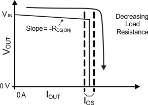
The TPD3S014-Q1 responds to overloads by limiting output current to the static current-limit (IOS) levels shown in the Electrical Characteristics: TJ = TA = 25°C table. When an overload condition is present, the device maintains a constant output current, with the output voltage determined by (IOS × RLOAD). Two possible overload conditions can occur.
The first overload condition occurs when either:
- The input voltage is first applied, enable is true, and a short circuit is present (load which draws IOUT > IOS) or
- The input voltage is present and the TPD3S014-Q1 is enabled into a short circuit.
The output voltage is held near zero potential with respect to ground and the TPD3S014-Q1 ramps the output current to IOS. The TPD3S014-Q1 limits the current to IOS until the overload condition is removed or the device begins to thermal cycle. The device subsequently cycles current off and on as the thermal protection engages.
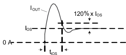
The second condition is when an overload occurs while the device is enabled and fully turned on. The device responds to the overload condition within tIOS when the specified overload (per Electrical Characteristics: TJ = TA = 25°C, Electrical Characteristics: –40°C ≤ TA ≤ 105°C tables) is applied (See Figure 8-3 and Figure 8-4). The response speed and shape varies with the overload level, input circuit, and rate of application. The current-limit response varies between simply settling to IOS, or turnoff and controlled return to IOS. Similar to the previous case, the TPD3S014-Q1 limits the current to IOS until the overload condition is removed or the device begins to thermal cycle.
 Figure 8-3 Output Short Circuit Parameters
 Figure 8-4 Output Characteristic Showing Current Limit
The TPD3S014-Q1 thermal cycles if an overload condition is present long enough to activate thermal limiting in any of the cases shown in Figure 8-3 and Figure 8-4. This is because of the relatively large power dissipation [(VIN – VOUT) × IOS] driving the junction temperature up. The devices turn off when the junction temperature exceeds 135°C (minimum) while in current limit. The devices remains off until the junction temperature cools down to 20°C and then restarts.
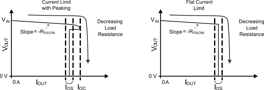
There are two kinds of current limit profiles typically available in TI switch products similar to the TPD3S014-Q1. Many older designs have an output I vs V characteristic similar to the plot labeled "Current Limit with Peaking" in Figure 8-5. This type of limiting can be characterized by two parameters, the current limit corner (IOC), and the short circuit current (IOS). IOC is often specified as a maximum value. The TPD3S014-Q1 part does not present noticeable peaking in the current limit, corresponding to the characteristic labeled "Flat Current Limit" in Figure 8-5. This is why the IOC parameter is not present in the Electrical Characteristics: TJ = TA = 25°C, Electrical Characteristics: –40°C ≤ TA ≤ 105°C tables.
 Figure 8-5 Current Limit Profiles