SLVSDK1C May   2016  – September 2017 TPS22990

PRODUCTION DATA.  

  1. Features
  2. Applications
  3. Description
  4. Revision History
  5. Device Comparison Table
  6. Pin Configuration and Functions
  7. Specifications
    1. 7.1 Absolute Maximum Ratings
    2. 7.2 ESD Ratings
    3. 7.3 Recommended Operating Conditions
    4. 7.4 Thermal Information
    5. 7.5 Electrical Characteristics—VBIAS = 5 V
    6. 7.6 Electrical Characteristics—VBIAS = 3.3 V
    7. 7.7 Switching Characteristics
    8. 7.8 Typical Characteristics
  8. Parameter Measurement Information
  9. Detailed Description
    1. 9.1 Overview
    2. 9.2 Functional Block Diagram
    3. 9.3 Feature Description
      1. 9.3.1 On and Off Control
      2. 9.3.2 Adjustable Rise Time
      3. 9.3.3 Power Good (PG)
      4. 9.3.4 Quick Output Discharge (QOD) (TPS22990 Only)
    4. 9.4 Device Functional Modes
  10. 10Application and Implementation
    1. 10.1 Application Information
      1. 10.1.1 Input to Output Voltage Drop
      2. 10.1.2 Input Capacitor
      3. 10.1.3 Thermal Consideration
      4. 10.1.4 PG Pull Up Resistor
      5. 10.1.5 Power Sequencing
      6. 10.1.6 Standby Power Reduction
    2. 10.2 Typical Application
      1. 10.2.1 Design Requirements
      2. 10.2.2 Detailed Design Procedure
        1. 10.2.2.1 Managing Inrush Current
      3. 10.2.3 Application Curves
  11. 11Power Supply Recommendations
  12. 12Layout
    1. 12.1 Layout Guidelines
    2. 12.2 Layout Example
  13. 13Device and Documentation Support
    1. 13.1 Documentation Support
      1. 13.1.1 Related Documentation
    2. 13.2 Receiving Notification of Documentation Updates
    3. 13.3 Community Resources
    4. 13.4 Trademarks
    5. 13.5 Electrostatic Discharge Caution
    6. 13.6 Glossary
  14. 14Mechanical, Packaging, and Orderable Information

Pin Configuration and Functions

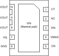
DML Package
10-Pin WSON
Top View
TPS22990 TPS22990_pinout_top_view.gif
DML Package
10-Pin WSON
Bottom View
TPS22990 TPS22990_pinout_bottom_view.gif

Pin Functions

PIN TYPE DESCRIPTION
NO. NAME
1 CT O VOUT slew rate control
2 NC Not internally connected
3 VIN I Switch input. Bypass this input with a ceramic capacitor to GND
4 VBIAS P Bias voltage. Power supply to the device
5 ON I Active high switch control input. Do not leave floating
6 GND GND Device ground
7 PG O Power good. Active high, open drain output. Tie to GND if not used
8 VOUT O Switch output
9
10
VIN (Thermal Pad) I Switch input. VIN and thermal pad (exposed center pad) to alleviate thermal stress. See the Layout section for layout guidelines