SLVSDM4D
November 2018 – December 2019
TPS1HA08-Q1
PRODUCTION DATA.
1
Features
2
Applications
3
Description
Simplified Schematic
4
Revision History
5
Device Comparison Table
6
Pin Configuration and Functions
Pin Functions
6.1
Recommended Connections for Unused Pins
7
Specifications
7.1
Absolute Maximum Ratings
7.2
ESD Ratings
7.3
Recommended Operating Conditions
7.4
Thermal Information
7.5
Electrical Characteristics
7.6
Switching Characteristics
7.7
SNS Timing Characteristics
7.8
Typical Characteristics
8
Parameter Measurement Information
9
Detailed Description
9.1
Overview
9.1.1
Device Nomenclature
9.2
Functional Block Diagram
9.3
Feature Description
9.3.1
Protection Mechanisms
9.3.1.1
Thermal Shutdown
9.3.1.2
Current Limit
9.3.1.2.1
Current Limit Foldback
9.3.1.2.2
Selectable Current Limit Threshold
9.3.1.2.3
Undervoltage Lockout (UVLO)
9.3.1.2.4
VBB during Short-to-Ground
9.3.1.3
Energy Limit
9.3.1.4
Voltage Transients
9.3.1.4.1
Load Dump
9.3.1.4.2
Driving Inductive and Capacitive Loads
9.3.1.5
Reverse Battery
9.3.1.6
Fault Event – Timing Diagrams
9.3.2
Diagnostic Mechanisms
9.3.2.1
VOUT Short-to-Battery and Open-Load
9.3.2.1.1
Detection With Switch Enabled
9.3.2.1.2
Detection With Switch Disabled
9.3.2.2
SNS Output
9.3.2.2.1
RSNS Value
9.3.2.2.1.1
High Accuracy Load Current Sense
9.3.2.2.1.2
SNS Output Filter
9.3.2.3
ST Pin
9.3.2.4
Fault Indication and SNS Mux
9.3.2.5
Resistor Sharing
9.3.2.6
High-Frequency, Low Duty-Cycle Current Sensing
9.3.3
Enable Watchdog
9.4
Device Functional Modes
9.4.1
Off
9.4.2
Standby
9.4.3
Diagnostic
9.4.4
Standby Delay
9.4.5
Active
9.4.6
Fault
10
Application and Implementation
10.1
Application Information
10.1.1
Ground Protection Network
10.1.2
Interface With Microcontroller
10.1.3
I/O Protection
10.1.4
Inverse Current
10.1.5
Loss of GND
10.1.6
Automotive Standards
10.1.6.1
ISO7637-2
10.1.6.2
AEC – Q100-012 Short Circuit Reliability
10.1.7
Thermal Information
10.2
Typical Application
10.2.1
Design Requirements
10.2.2
Detailed Design Procedure
10.2.2.1
Thermal Considerations
10.2.2.2
Diagnostics
10.2.2.2.1
Selecting the RISNS Value
10.2.3
Application Curves
11
Power Supply Recommendations
12
Layout
12.1
Layout Guidelines
12.2
Layout Example
13
Device and Documentation Support
13.1
Device Support
13.1.1
Related Documentation
13.2
Trademarks
13.3
Electrostatic Discharge Caution
13.4
Glossary
14
Mechanical, Packaging, and Orderable Information
12.2
Layout Example
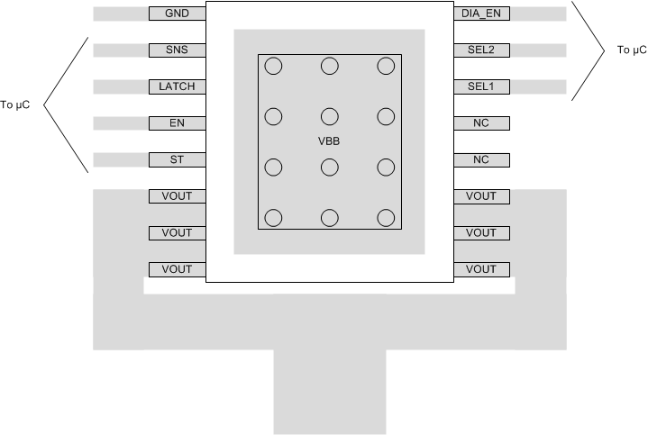
Figure 61.
PWP Layout Example