SLVSDO2C February   2017  – February 2018 TVS3300

PRODUCTION DATA.  

  1. Features
  2. Applications
  3. Description
    1.     Device Images
      1.      Footprint Comparison
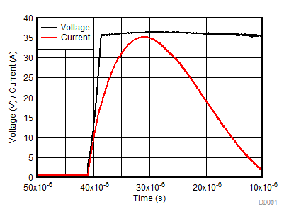
      2.      Voltage Clamp Response to 8/20 µs Surge Event
  4. Revision History
  5. Device Comparison Table
  6. Pin Configuration and Functions
    1.     Pin Functions
  7. Specifications
    1. 7.1 Absolute Maximum Ratings
    2. 7.2 ESD Ratings - JEDEC
    3. 7.3 ESD Ratings - IEC
    4. 7.4 Recommended Operating Conditions
    5. 7.5 Thermal Information
    6. 7.6 Electrical Characteristics
    7. 7.7 Typical Characteristics
  8. Detailed Description
    1. 8.1 Overview
    2. 8.2 Functional Block Diagram
    3. 8.3 Feature Description
    4. 8.4 Reliability Testing
    5. 8.5 Device Functional Modes
      1. 8.5.1 Protection Specifications
      2. 8.5.2 Minimal Derating
      3. 8.5.3 Transient Performance
  9. Application and Implementation
    1. 9.1 Application Information
    2. 9.2 Typical Application
      1. 9.2.1 Design Requirements
      2. 9.2.2 Detailed Design Procedure
      3. 9.2.3 PLC Surge Protection Reference Design
      4. 9.2.4 Configuration Options
  10. 10Power Supply Recommendations
  11. 11Layout
    1. 11.1 Layout Guidelines
    2. 11.2 Layout Example
  12. 12Device and Documentation Support
    1. 12.1 Documentation Support
      1. 12.1.1 Related Documentation
    2. 12.2 Receiving Notification of Documentation Updates
    3. 12.3 Community Resources
    4. 12.4 Trademarks
    5. 12.5 Electrostatic Discharge Caution
    6. 12.6 Glossary
  13. 13Mechanical, Packaging, and Orderable Information

Typical Characteristics

TVS3300 D001_SLVSDO2.gif
Figure 1. 8/20 µs Surge Response at 35 A
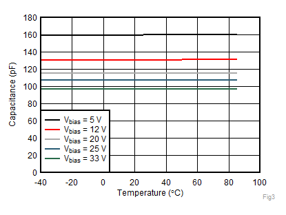
TVS3300 Fig3_TVS3300.gif
f = 1 MHz, 30 mVpp, IO to GND
Figure 3. Capacitance vs Temperature Across Bias
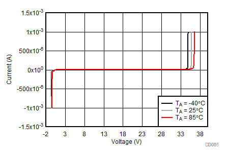
TVS3300 D005_SLVSDO2.gif
Figure 5. I/V Curve Across Temperature
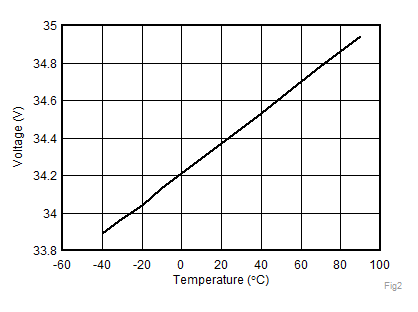
TVS3300 Fig2_TVS3300.gif
Figure 7. Breakdown Voltage (1 mA) vs Temperature
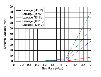
TVS3300 D009_SLVSED2.gif
Figure 9. Dynamic Leakage vs Signal Slew Rate across Temperature
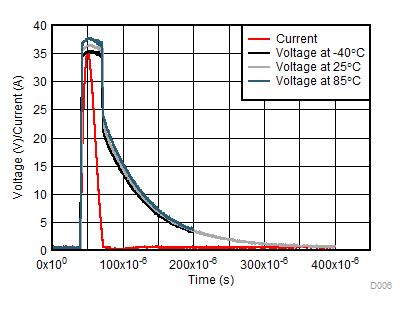
TVS3300 D006_SLVSDO2.gif
Figure 2. 8/20 µs Surge Response at 35 A Across Temperature
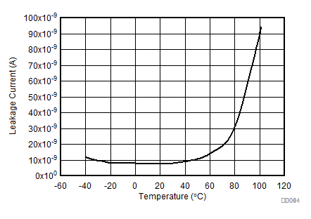
TVS3300 D004_SLVSDO2.gif
Figure 4. Leakage Current vs Temperature at 33 V
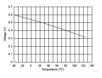
TVS3300 D006_SLVSED2_2.gif
Figure 6. Forward Voltage vs Temperature
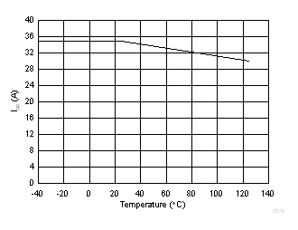
TVS3300 D016_SLVSD02.gif
Figure 8. Max Surge Current (8/20 µs) vs Temperature