SLVSDR3C may 2018 – may 2023 ADC12DL3200
PRODUCTION DATA
- 1
- 1Features
- 2Applications
- 3Description
- 4Revision History
- 5Pin Configuration and Functions
-
6Specifications
- 6.1 Absolute Maximum Ratings
- 6.2 ESD Ratings
- 6.3 Recommended Operating Conditions
- 6.4 Thermal Information
- 6.5 Electrical Characteristics: DC Specifications
- 6.6 Electrical Characteristics: Power Consumption
- 6.7 Electrical Characteristics: AC Specifications (Dual-Channel Mode)
- 6.8 Electrical Characteristics: AC Specifications (Single-Channel Mode)
- 6.9 Timing Requirements
- 6.10 Switching Characteristics
- 6.11 Typical Characteristics
-
7Detailed Description
- 7.1 Overview
- 7.2 Functional Block Diagram
- 7.3
Feature Description
- 7.3.1 Analog Inputs
- 7.3.2 ADC Core
- 7.3.3 Timestamp
- 7.3.4 Clocking
- 7.3.5 LVDS Digital Interface
- 7.3.6 Alarm Monitoring
- 7.3.7 Temperature Monitoring Diode
- 7.3.8 Analog Reference Voltage
- 7.4
Device Functional Modes
- 7.4.1 Dual-Channel Mode (Non-DES Mode)
- 7.4.2 Internal Dither Modes
- 7.4.3 Single-Channel Mode (DES Mode)
- 7.4.4 LVDS Output Driver Modes
- 7.4.5 LVDS Output Modes
- 7.4.6 Power-Down Modes
- 7.4.7 Calibration Modes and Trimming
- 7.4.8 Offset Calibration
- 7.4.9 Trimming
- 7.5 Programming
- 7.6 Register Maps
- Application and Implementation
- 8Device and Documentation Support
- 9Mechanical, Packaging, and Orderable Information
7.4.7 Calibration Modes and Trimming
The ADC12DL3200 has two calibration modes available: foreground calibration and background calibration. When foreground calibration is initiated the ADCs are automatically taken offline and the output data become mid-code (0x000 in 2's complement) while a calibration is occurring. Background calibration allows the ADC to continue normal operation while the ADC cores are calibrated in the background by swapping in a different ADC core to take its place. Additional offset calibration features are available in both foreground and background calibration modes. Further, a number of ADC parameters can be trimmed to optimize performance in a user system.
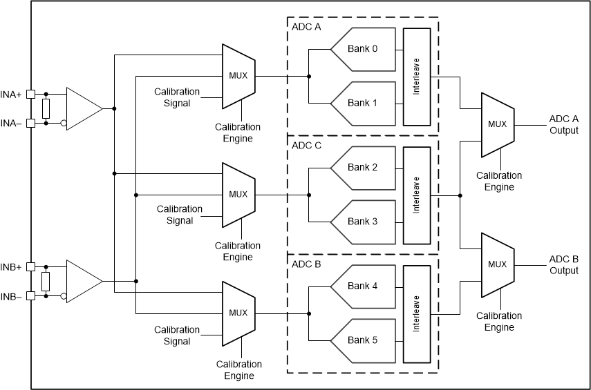
The ADC12DL3200 consists of a total of six sub-ADCs, each referred to as a bank, with two banks forming an ADC core. The banks sample out-of-phase so that each ADC core is two-way interleaved. The six banks form three ADC cores, referred to as ADC A, ADC B, and ADC C. In foreground calibration mode, ADC A samples INA± and ADC B samples INB± in dual-channel mode and both ADC A and ADC B sample INA± (or INB±) in single-channel mode. In the background calibration modes, the third ADC core, ADC C, is swapped in periodically for ADC A and ADC B so that they can be calibrated without disrupting operation.
Figure 7-4 shows a diagram of the calibration system including labeling of the banks that make up each ADC core. When calibration is performed the linearity, gain, and offset voltage for each bank are calibrated to an internally generated calibration signal. The analog inputs can be driven during calibration, both foreground and background, except that when offset calibration (see CAL_OS and CAL_BGOS in the CAL_CFG0 register) is used there must be no signals (or aliased signals) near DC for proper estimation of the offset (see the Section 7.4.8 section).
 Figure 7-4 ADC12DL3200 Calibration System Block Diagram
In addition to calibration, a number of ADC parameters are user-controllable to provide trimming for optimal performance. These parameters include input offset voltage, ADC gain, interleaving timing, and input termination resistance. The default trim values are programmed at the factory to unique values for each device that are determined to be optimal at the test system operating conditions. The factory-programmed values can be read from the trim registers and adjusted as desired. The register fields that control the trimming are labeled according to the input that is being sampled (INA± or INB±), the bank that is being trimmed, or the ADC core that is being trimmed. Trim values are not expected to change as operating conditions change, however optimal performance can be obtained by doing so. Any custom trimming must be done on a per device basis because of process variations, meaning that there is no global optimal setting for all parts. See the Section 7.4.9 section for information about the available trim parameters and associated registers.