SLVSDZ4D February 2018 – February 2020 TPS2HB35-Q1
PRODUCTION DATA.
- 1 Features
- 2 Applications
- 3 Description
- 4 Revision History
- 5 Device Comparison Table
- 6 Pin Configuration and Functions
- 7 Specifications
- 8 Parameter Measurement Information
-
9 Detailed Description
- 9.1 Overview
- 9.2 Functional Block Diagram
- 9.3
Feature Description
- 9.3.1 Protection Mechanisms
- 9.3.2 Diagnostic Mechanisms
- 9.4 Device Functional Modes
- 10Application and Implementation
- 11Power Supply Recommendations
- 12Layout
- 13Device and Documentation Support
- 14Mechanical, Packaging, and Orderable Information
9.3.1.2 Current Limit
When IOUT reaches the current limit threshold, ICL, the channel will switch off immediately. The ICL value will vary with slew rate and a fast current increase that occurs during a powered-on short circuit can temporarily go above the specified ICL value. In the case that the device remains enabled (and limits IOUT), the thermal shutdown protection feature may be triggered due to the high amount of power dissipation in the device. When the switch is in the FAULT state it will output an output current ISNSFH on the SNS pin. In addition, fault indication will occur when the switch is actively limiting current (applicable to version C).
During a short circuit event, the device will hit the ICL value that is listed in the Electrical Characteristics table (for the given device version and RILIM) and then turn the output off or regulate the output current to protect the device. The device will register a short circuit event when the output current exceeds ICL, however the measured maximum current may exceed the ICL value due to the TPS2HB35-Q1 deglitch filter and turn-off time. The device is specified to protect itself during a short circuit event over the nominal supple voltage range (as defined in the Electrical Characteristics table) at 125°C.
The current limit specification in the datasheet is based on the part being enabled into a short circuit condition with 5-µH inductor on the input and output and the input resistance being less than 10 mΩ and the output impedance less than 100 mΩ. When the part is enabled into this short circuit condition, the current will rise up to the threshold specified in the Electrical Characteristics table before it begins to shut off the current. The deglitch filter time for the device to react to the current threshold is 3 µs. Therefore if you take Version A/B and subtract 3 µs from the maximum current value, the current limit threshold will align with the value specified in the Electrical Characteristics table.
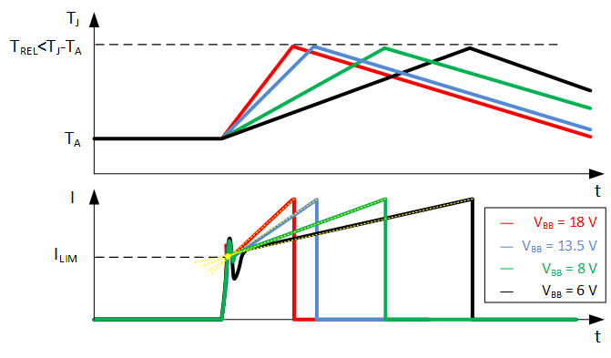
The current threshold is defined for version C is different than version A or B. For version C, the current through the device continues to flow until the device hits relative thermal shutdown (TREL). For different VBB's the slope of the current will change. Therefore the intersection point of where each of the slopes for the different VBB values is determined as the current threshold, ILIM, as shown in Figure 37. This behavior allows for the TPS2HB35C-Q1 to be able to charge up a 270 µF capacitor without shutting off due to hitting the current limit as versions A and B would.
 Figure 37. Version C Current Threshold Definition
 The maximum point that the current can reach to is bound in the Electrical Characteristics table. This worst case value is based on an extremely low impedance short and the current at which TREL is finally reached.