SLVSE13J September   2017  – November 2024 TLV7031 , TLV7032 , TLV7034 , TLV7041 , TLV7042 , TLV7044

PRODUCTION DATA  

  1.   1
  2. Features
  3. Applications
  4. Description
  5. Pin Configuration and Functions
    1. 4.1 Pin Functions: TLV7031/41 Singles including "S" and "L" options
    2. 4.2 Pin Functions: TLV7032/42 Dual
    3. 4.3 Pin Functions: TLV7034/44 Quad
  6. Specifications
    1. 5.1  Absolute Maximum Ratings
    2. 5.2  ESD Ratings
    3. 5.3  Recommended Operating Conditions
    4. 5.4  Thermal Information (Single)
    5. 5.5  Thermal Information (Dual)
    6. 5.6  Thermal Information (Quad)
    7. 5.7  Electrical Characteristics (Single)
    8. 5.8  Switching Characteristics (Single)
    9. 5.9  Electrical Characteristics (Dual)
    10. 5.10 Switching Characteristics (Dual)
    11. 5.11 Electrical Characteristics (Quad)
    12. 5.12 Switching Characteristics (Quad)
    13. 5.13 Timing Diagrams
    14. 5.14 Typical Characteristics
  7. Detailed Description
    1. 6.1 Overview
    2. 6.2 Functional Block Diagram
    3. 6.3 Feature Description
    4. 6.4 Device Functional Modes
      1. 6.4.1 Inputs
      2. 6.4.2 Internal Hysteresis
      3. 6.4.3 Output
  8. Application and Implementation
    1. 7.1 Application Information
      1. 7.1.1 Inverting Comparator With Hysteresis for TLV703x
      2. 7.1.2 Non-Inverting Comparator With Hysteresis for TLV703x
    2. 7.2 Typical Applications
      1. 7.2.1 Window Comparator
        1. 7.2.1.1 Design Requirements
        2. 7.2.1.2 Detailed Design Procedure
        3. 7.2.1.3 Application Curve
      2. 7.2.2 IR Receiver Analog Front End
        1. 7.2.2.1 Design Requirements
        2. 7.2.2.2 Detailed Design Procedure
        3. 7.2.2.3 Application Curve
      3. 7.2.3 Square-Wave Oscillator
        1. 7.2.3.1 Design Requirements
        2. 7.2.3.2 Detailed Design Procedure
        3. 7.2.3.3 Application Curve
      4. 7.2.4 Quadrature Rotary Encoder
        1. 7.2.4.1 Design Requirements
        2. 7.2.4.2 Detailed Design Procedure
        3. 7.2.4.3 Application Curve
    3. 7.3 Power Supply Recommendations
    4. 7.4 Layout
      1. 7.4.1 Layout Guidelines
      2. 7.4.2 Layout Example
  9. Device and Documentation Support
    1. 8.1 Device Support
      1. 8.1.1 Development Support
        1. 8.1.1.1 Evaluation Module
    2. 8.2 Documentation Support
      1. 8.2.1 Related Documentation
    3. 8.3 Receiving Notification of Documentation Updates
    4. 8.4 Support Resources
    5. 8.5 Trademarks
    6. 8.6 Electrostatic Discharge Caution
    7. 8.7 Glossary
  10. Revision History
  11. 10Mechanical, Packaging, and Orderable Information

Application Curve

Figure 7-9 shows the simulated results of an oscillator using the following component values:

  • R1 = R2 = R3 = R4 = 100kΩ
  • C1 = 100pF, CL = 20pF
  • V+ = 5V, V– = GND
  • Cstray (not shown) from VA to GND = 10pF
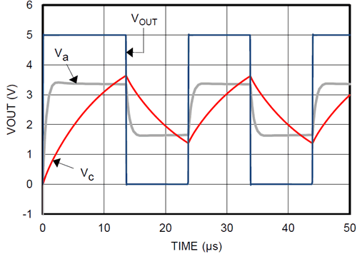
TLV7031 TLV7032 TLV7041 TLV7042 TLV7034 TLV7044 Square-Wave Oscillator Output WaveformFigure 7-9 Square-Wave Oscillator Output Waveform