SLVSE31C January   2018  – July 2018 TPSM84209

PRODUCTION DATA.  

  1. Features
  2. Applications
  3. Description
    1.     Device Images
      1.      Simplified Application
      2.      Efficiency vs Output Current
  4. Revision History
  5. Pin Configuration and Functions
    1.     Pin Functions
  6. Specifications
    1. 6.1 Absolute Maximum Ratings
    2. 6.2 ESD Ratings
    3. 6.3 Recommended Operating Conditions
    4. 6.4 Thermal Information
    5. 6.5 Electrical Characteristics
    6. 6.6 Typical Characteristics (VIN = 5 V)
    7. 6.7 Typical Characteristics (VIN = 12 V)
    8. 6.8 Typical Characteristics (VIN = 24 V)
  7. Detailed Description
    1. 7.1 Overview
    2. 7.2 Functional Block Diagram
    3. 7.3 Feature Description
      1. 7.3.1  Adjusting the Output Voltage
      2. 7.3.2  Input Capacitor Selection
      3. 7.3.3  Undervoltage Lockout (UVLO)
      4. 7.3.4  Output Capacitor Selection
      5. 7.3.5  Feed-Forward Capacitor
      6. 7.3.6  Operating Range
      7. 7.3.7  Output Current Rating
      8. 7.3.8  Enable (EN)
      9. 7.3.9  Internal Soft Start
      10. 7.3.10 Safe Start-Up Into Prebiased Outputs
      11. 7.3.11 Light Load Efficiency / Eco-Mode
      12. 7.3.12 Voltage Dropout
      13. 7.3.13 Overcurrent Protection
      14. 7.3.14 Output Overvoltage Protection (OVP)
      15. 7.3.15 Thermal Performance
      16. 7.3.16 Thermal Shutdown
    4. 7.4 Device Functional Modes
      1. 7.4.1 Active Mode
      2. 7.4.2 Eco-Mode Operation
      3. 7.4.3 Shutdown Mode
  8. Application and Implementation
    1. 8.1 Application Information
    2. 8.2 Typical Application
      1. 8.2.1 Design Requirements
      2. 8.2.2 Detailed Design Procedure
        1. 8.2.2.1 Custom Design With WEBENCH® Tools
        2. 8.2.2.2 Output Voltage Setpoint
        3. 8.2.2.3 Input Capacitors
        4. 8.2.2.4 Output Capacitors
        5. 8.2.2.5 Enable Control
      3. 8.2.3 Application Waveforms
  9. Power Supply Recommendations
  10. 10Layout
    1. 10.1 Layout Guidelines
    2. 10.2 Layout Examples
    3. 10.3 EMI
      1. 10.3.1 EMI Plots
    4. 10.4 Package Specifications
  11. 11Device and Documentation Support
    1. 11.1 Device Support
      1. 11.1.1 Third-Party Products Disclaimer
    2. 11.2 Custom Design With WEBENCH® Tools
    3. 11.3 Receiving Notification of Documentation Updates
    4. 11.4 Community Resources
    5. 11.5 Trademarks
    6. 11.6 Electrostatic Discharge Caution
    7. 11.7 Glossary
  12. 12Mechanical, Packaging, and Orderable Information
    1. 12.1 Tape and Reel Information

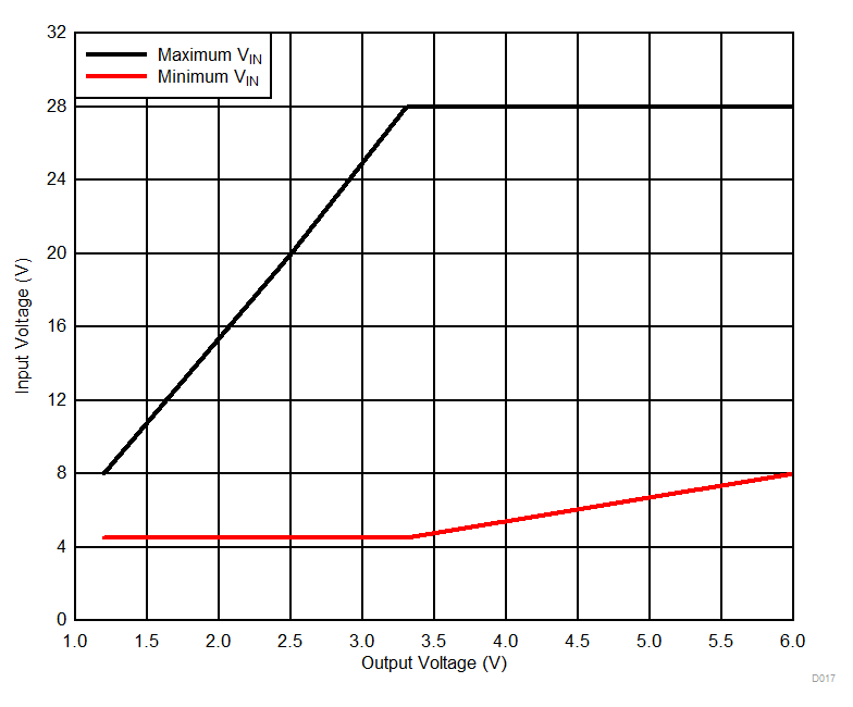
Operating Range

The TPSM84209 operates over a wide input voltage and output voltage range; however, not all output voltages can operate over the entire input voltage range. The maximum and minimum input voltage limits are shown in Figure 20. The TPSM84209 can be operated between the Maximum and Minimum VIN limit lines.

Operating above the Maximum VIN line may cause the device to skip pulses in order to maintain the regulated output voltage.
TPSM84209 D017_MaxMinVin3.gifFigure 20. Input Voltage vs Output Voltage