SLVSE84D December 2017 – July 2021 TLV767
PRODUCTION DATA
- 1 Features
- 2 Applications
- 3 Description
- 4 Revision History
- 5 Pin Configuration and Functions
- 6 Specifications
- 7 Typical Characteristics
- 8 Detailed Description
- 9 Application and Implementation
- 10Power Supply Recommendations
- 11Layout
- 12Device and Documentation Support
3 Description
The TLV767 is a wide input linear voltage regulator supporting an input voltage range from 2.5 V to 16 V and up to 1 A of load current. The output range is from 0.8 V to 6.6 V or up to 14.6 V in the adjustable version.
Additionally, the TLV767 has a 1% output accuracy that can meet the needs of low voltage microcontrollers (MCUs) and processors.
The TLV767 is designed to have a much lower IQ than traditional wide-VIN regulators, thus making the device well positioned to meet the needs of increasingly stringent standby power requirements. When disabled, the TLV767 draws only 1.5 µA of IQ.
The internal soft-start time and foldback current limit reduce inrush current during start up, thus minimizing input capacitance.
Wide bandwidth PSRR performance is greater than 70 dB at 1 kHz and 46 dB at 1 MHz, which helps attenuate the switching frequency of an upstream DC/DC converter and minimizes post regulator filtering. To allow for more flexibility, the TLV767 has both fixed and adjustable versions.
The TLV767 is available in a 6-pin, 2-mm × 2-mm WSON (DRV), an 8-pin 3-mm x 3-mm HVSSOP (DGN), and a 5-pin 2.9-mm x 1.6-mm SOT-23 (DBV) package.
| PART NUMBER | PACKAGE | BODY SIZE (NOM) |
|---|---|---|
| TLV767 | WSON (6) | 2.00 mm × 2.00 mm |
| HVSSOP (8) | 3.00 mm x 3.00 mm | |
| SOT-23 (5) | 2.90 mm x 1.60 mm |
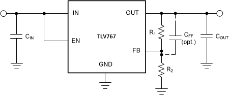
 Typical Application Circuit